

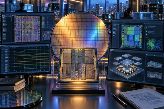
The September release covers more than A14. According to Cadence's announcement, carried in full by Wccftech, Cadence has achieved tool certification for TSMC's advanced A14 process, demonstrated an industry-leading UALink solution in TSMC N3P, and introduced new silicon-proven IP for N3P and N2P technologies. It also extends Cadence's design support for TSMC's 3DFabric advanced packaging to wafer-scale systems. Investor coverage from Seeking Alpha and GuruFocus confirms the timing and the headline A14 and N2P certifications. GuruFocus reports that following the news, CDNS shares rose approximately 2.64% to around $310.76.
Cadence's TSMC A14 Certification Moves From "Ongoing Collaboration" to Certified Flows
Put simply, certification is TSMC's approval that a vendor's tools produce results that match the foundry's process requirements. TSMC's EDA Alliance page says the program validates partner tools and methodologies against new process technologies. Its advanced-node categories include automated place-and-route, library characterization, timing and power signoff, electromigration and IR-drop analysis, physical verification (DRC, LVS and dummy fill), RC extraction, circuit simulators and thermal analysis. The same page lists A14, A16, N2P and N3C as the core of the current program, with Cadence, Siemens EDA and Synopsys as the major participants.
The before and after is easy to see. In April 2026, Cadence described its tools as all certified for TSMC N2 and A16, and ongoing collaboration for A14 PDKs to accelerate convergence of tapeout-quality results for AI/HPC applications. Five months later, the company says its digital full flow, signoff flow and custom/analog flows are certified for both A16 and A14.
The certified digital flow for A14 and A16 includes:
- The Innovus Implementation System handles physical implementation, and Cadence Cerebrus Intelligent Chip Explorer is used for design-technology co-optimization (DTCO).
- The Tempus Timing and ECO Solution, Voltus IC Power Integrity Solution and Quantus Extraction Solution cover timing, power integrity and parasitic extraction.
- The Pegasus Verification System, EMX Planar 3D Solver and Liberate Characterization Portfolio cover verification, electromagnetic modeling and cell characterization.
- The Genus Synthesis Solution is described as "enabled" rather than certified, the same wording Cadence used for Genus in April.
One detail is worth knowing for anyone who checks TSMC's own records. The foundry's public A14 status table is dated July 10, 2026, and marks each category as either certified or work in progress. It predates the September announcement, so any gaps it shows reflect July, not a conflict with Cadence's later claim.
A14 itself is still a future node. When TSMC introduced it in 2025, All About Circuits reported that A14 was expected to enter production in 2028 and delivers up to 15% speed improvement or 30% power reduction at equivalent performance, along with a 20% logic density boost. Those are TSMC's figures from its launch. Certifying tools in late 2026 fits the usual sequence: design tools have to be qualified long before chips can be taped out and built at volume.
Where the 2.5X Virtuoso Migration Claim Actually Applies
The 2.5X headline number is narrow. It comes from Cadence's custom and analog tools. The company says Virtuoso Studio now offers design-rule-correct layout generation and automated design migration to TSMC A16 and A14, "reducing iterations by up to 2.5X and improving first-pass success for AI, HPC and mobile SoCs." Cadence gave no test designs, baseline or methodology for the figure. Treat it as a best-case vendor number for one step of the design flow.
It helps to know why analog migration is a pain point. Digital logic can mostly be resynthesized for a new node by automated tools. Analog blocks such as PLLs, data converters and I/O circuits are usually hand-tuned layouts. TSMC's own reference-flow documentation says conventional analog porting "requires manual migration and verification on each design step," and describes the process as tedious and time-consuming. Its Analog Design Migration Reference Flow speeds up schematic migration, layout reuse and circuit optimization so proven analog blocks can be reused across nodes. Cadence's 2.5X claim sits inside that effort.
The "agentic AI" wording in the headline comes from the wider partnership. In April, Cadence said it was developing "agent‑ready" digital and analog flows that integrate agentic AI to enable goal‑driven PPA, reliability and productivity optimization. Engineering.com reported at the time that Cadence has embedded agentic AI in Virtuoso Studio flows with circuit optimization for TSMC process technologies. This includes the enablement for N2-to-A14 Analog Design Migration flow. The September release says the companies are "enabling agentic AI chip and 3D-IC design flows" across N3, N2, A16 and A14. It gives no measured result from agent-driven automation, so the only number on the table is the 2.5X migration figure.
Cadence's TSMC A14 IP Is Mostly Still in Development Until Q4 2026
Certified tools are only half of what a chip team needs. The other half is licensed IP: pre-designed, pre-validated blocks such as memory controllers, PHYs and standard-cell libraries. On A14, Cadence's IP is at an early stage. Per the release, UCIe-64G has been taped out on TSMC A14, LPDDR6 IP is in development, and a wide selection of HPC & AI memory IP and other protocols needed for compute chiplets have been prioritized for development. UCIe is the open die-to-die interconnect standard used to link chiplets.
The basic building blocks are due by the end of the year. Artisan Foundation IP and mixed‑signal IP for TSMC A14 are also in development and are expected to be available in Q4 2026, including standard cells, GPIO, and Memory Compilers for HPC/AI and networking applications. The "prioritized" memory and protocol IP has no delivery dates.
| Node | Cadence tool status (per Sept. 23 release) | IP status |
|---|---|---|
| A14 | Digital full flow, signoff and custom/analog certified | UCIe-64G taped out; LPDDR6 in development; Artisan Foundation and mixed-signal IP expected Q4 2026 |
| A16 | Digital full flow, signoff and custom/analog certified | Design-rule-correct layout and automated migration in Virtuoso |
| N2P | Analog, digital and signoff certified | DDR5, LPDDR5, PCIe 6.0 taped out; PCIe 3.0 tape-out expected Q4 2026; UCIe-64G in lab |
| N3P | Flows enabled as part of N3 family | UALink demonstrated; UCIe-64G characterized |
"Taped out" means a design has been sent to the fab for manufacturing. It does not mean the silicon has been tested, characterized and made available to license. On A14, only one IP block has reached tape-out.
N2P and N3P Carry the Silicon-Proven Half of the Cadence Announcement
The more mature IP is on the current 2nm and 3nm-class nodes. Cadence analog, digital, and signoff tool flows have been certified for TSMC N2P. Cadence also says the Virtuoso Layout Suite has added enhanced connectivity models, providing a production-ready custom design environment for quicker design starts. Its N2P IP is further along than its A14 IP: taped-out N2P IP includes DDR5, LPDDR5, and PCIe 6.0, with PCIe 3.0 IP expected to tape out in Q4 2026.
UCIe-64G is at a different stage on each node, and they are easy to confuse. It has taped out on A14, it is in the test lab as N2P silicon, and it has been characterized on N3P. Characterized means measured on real silicon. So N3P is the only node where Cadence reports measured UCIe-64G results. The N2P version has not finished lab testing, and the A14 version has only been sent to the fab.
N3P also hosts the UALink demonstration. UALink is an accelerator-to-accelerator interconnect standard for linking AI chips inside a server pod. Cadence calls its demo "industry-leading" but published no bandwidth, latency or power figures. The release also lists a broader HPC/AI IP portfolio covering HBM4/4E, LPDDR6/5X, DDR5-MRDIMM, PCIe 7.0 and UCIe 64G, without saying which nodes each block is available on.
The only customer named is Global Unichip Corp. (GUC), a TSMC-affiliated custom-silicon design house. GUC says it uses Cadence tools for AI accelerators and hyperscale systems. Senior vice president Louis Lin said Cadence's tools provide "the predictability, performance, and silicon correlation" GUC needs to tape out complex designs. His comments refer to N3P and N2P. Neither GUC nor the release names a GUC chip or claims a GUC tape-out on A14.
3DFabric, SoW-X and TSMC-COUPE Push Cadence Tools Toward Wafer-Scale AI Systems
The packaging section is where the announcement looks furthest ahead. Cadence says its tools support the full design flow for TSMC SoW-X, TSMC's system-on-wafer packaging, with "hundreds of chiplets and millions of bumps." They also support 5X-reticle-size CoWoS-L-style packages. A reticle is the largest area a lithography tool can expose in one pass, so a package five times that size carries far more silicon than any single die could.
Cadence's Integrity 3D-IC platform handles system planning and assembly. It can integrate SoIC die stacks, eDTC, MIMCap capacitors, integrated voltage regulators (IVR), HBM logic base dies and substrates. A pre-simulation-driven die-to-die auto-routing flow is now certified with the Cadence Allegro Substrate Router and OmniRoute Advanced Interconnect Router. According to the release, the flow automatically works out signal-integrity-optimized routing across CoWoS architectures while meeting UCIe requirements.
Cadence has been working toward this for some time. When TSMC first introduced A14 in 2025, All About Circuits noted that TSMC's roadmap extended to advanced packaging with chip-on-wafer-on-substrate (CoWoS), its compact universal photonic engine (COUPE), and high-bandwidth memory support. The September release adds that TSMC-COUPE's photonic-to-silicon connectivity is now enabled for integration with Cadence's 224G SerDes IP. Cadence describes that SerDes as aligned with UALink, ESUN, UltraEthernet and co-packaged optics (CPO).
All of this is design enablement. It means Cadence's tools can model and assemble these structures. The release does not say any customer has used these flows to build a production wafer-scale system.
What the Cadence–TSMC A14 Milestone Means for PC and IT Buyers
This announcement calls for no action from Windows users or IT administrators. Nothing ships, and nothing changes in the PCs, servers or cloud instances you can buy in 2026. It is a timeline signal. Leading-edge chip design depends on qualified tools, and Cadence now says those tools exist for A14. TSMC's own table from July also shows Synopsys and Siemens EDA in the program, so A14 design work can move from exploration toward real tape-outs across the industry.
For anyone planning hardware refreshes, the practical point is timing. A14 volume production is expected in 2028, so products built on it would arrive after that. Which PC or datacenter chips will use A14 is not disclosed anywhere in this announcement, and it would be speculation to name any. The nearer-term signal is N2P. Certified flows plus taped-out DDR5, LPDDR5 and PCIe 6.0 IP point to where custom AI and HPC silicon is being built now.
- Cadence says its digital full flow, signoff and custom/analog flows are certified for TSMC A14 and A16 as of September 23, 2026, up from "ongoing collaboration" on A14 in April.
- The "up to 2.5X" figure applies only to iterations in Virtuoso Studio's automated custom/analog migration to A16 and A14, and Cadence published no benchmark behind it.
- On A14, only UCIe-64G IP has taped out, while standard cells, GPIO, memory compilers and mixed-signal IP are expected in Q4 2026.
- On N2P, DDR5, LPDDR5 and PCIe 6.0 IP have taped out, and PCIe 3.0 is due to tape out in Q4 2026.
- TSMC's public A14 certification table is dated July 10, 2026, so it does not yet reflect the September announcement.
- A14 volume production is expected in 2028, so none of this changes hardware you can buy before then.
Cadence's A14 certification is a real milestone. It turns TSMC's next full node from a research target into something chip teams can start committing designs to. The foundation IP due in Q4 2026 is what those teams need to start real A14 layouts, and the first shipping A14 silicon would follow TSMC's 2028 production start.