

Intel–AUO reporting points toward chip packaging first
The reported Intel–AUO talks sit at the intersection of two manufacturing disciplines: processing glass for displays and packaging semiconductor components. DIGITIMES describes display manufacturers seeking to turn their large-area glass-processing expertise into advanced-packaging capabilities, with Intel reportedly discussing microLED substrate technology with AUO. Its stated targets are co-packaged optics, abbreviated CPO, and high-density computing.
That description gives the development a different emphasis from the consumer-display interpretation. PC Gamer, citing Taiwan’s Economic Daily, presented the collaboration as a possible route to more accessible microLED panels. It suggested that embedding electronics in glass could integrate a display-control chip into the panel, bringing packaging and cost advantages.
There is a plausible engineering connection between those ideas, but they are separate propositions. A manufacturer’s expertise in glass can be useful for semiconductor packaging without the resulting product becoming a screen. Likewise, work involving micro light-emitting diodes does not automatically establish a program to manufacture millions of individually controlled display pixels.
MicroLED-info also reports that Intel is discussing advanced CPO or microLED-based optical input/output with AUO, attributing that information to Taiwanese reporting. Its account therefore reinforces the packaging interpretation, but should not be counted as independent confirmation of an agreement. The available reporting establishes reported talks, rather than a jointly announced product or a confirmed manufacturing contract.
For readers following future PC displays, the important change is the reported possibility of cooperation between Intel and AUO. The claim that this cooperation will make consumer microLED monitors affordable goes substantially further than the evidence.
Intel’s microLED patent embeds emitters, not a promised monitor controller
Intel’s patent application US20240079530A1, titled “IC Package with Micro LEDs,” was filed on September 6, 2022, and published on March 7, 2024. Its technical description is useful because it shows what “embedding a semiconductor chip within glass” means in this particular invention.
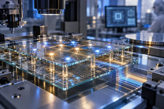
The semiconductor die—the piece of semiconductor material inside the package—contains microLEDs. A glass substrate surrounds at least part of that die, while conductive connections called through-glass vias, or TGVs, carry electrical connections through the glass. Other package substrates connect those structures to the surrounding electronics.
In one illustrated arrangement, the patent describes power travelling from a motherboard through connections in a package substrate and then through the glass to the light-emitting die. Other conductive structures distribute input and output signals. Glass is therefore part of the package’s electrical and physical construction, rather than simply a transparent cover over a display.
This is where the monitor interpretation needs a correction. PC Gamer suggested that the embedded semiconductor chip would be a display-control chip integrated into a microLED panel. Intel’s described die instead contains the microLED emitters themselves. The record does not establish the claimed display-controller integration.
The patent includes several arrangements, with different positions for the die and its connections:
- One arrangement partially embeds the light-emitting die in glass while leaving its back surface exposed.
- Another fully embeds the die in glass and changes its orientation within the package.
- A further arrangement embeds the die in a neighbouring package substrate and uses mirrors to direct emitted light through the glass and out of the package.
These are substantive packaging proposals. They describe ways to place, power and expose light-emitting components within an integrated assembly. They do not provide a monitor specification, a panel-production cost or a measured improvement over an existing display-manufacturing process.
The patent’s stated uses are especially revealing. Its background discusses decorative lighting and operation indicators in electronic devices. The detailed description explicitly proposes aesthetic components, electrical-test indicators and illuminated wording across a CPU.
There is also a broader electronic-device example that mentions microLED display panels, notebooks, televisions and monitors. That means it would be too categorical to say the document has no display connection. Nevertheless, listing devices that might incorporate an invention is different from documenting a complete high-resolution panel architecture.
Nor does the patent itself establish an AUO relationship. Intel’s published technical work and the reported talks are two distinct pieces of evidence; neither should be used to quietly certify the other.
Through-glass vias provide a mechanism, not evidence of lower panel prices
The fabrication description gives the story more substance than a vague prediction about future displays. Intel outlines creating cavities in glass through laser treatment and etching, forming conductive structures through electroplating and planarization, and making space for the semiconductor die.
In one sequence, a cavity shaped for the die is prepared alongside the openings used for electrical connections. Conductive material is deposited and subsequently removed from the die cavity, after which the die is inserted. Silicon nitride layers and package substrates complete the illustrated assembly.
A separate sequence places the die against the glass and connects its contacts to the TGVs before applying a dielectric moulding material. That material surrounds the die to form part of the package. The patent thus describes more than one route to combining glass, electrical routing and emitters.
Those details explain why glass-processing expertise could be relevant to a semiconductor-packaging collaboration. They also show why “Intel has a patent” cannot stand in for “Intel has solved microLED manufacturing costs.” A proposed assembly sequence supplies no production-throughput figures, commercial yield measurements or cost comparison.
The distinction is practical. Yield is the proportion of manufactured units that meet the required specification. Without results showing how reliably an assembly can be produced, its apparent integration advantages cannot be translated into a retail-price reduction.
The same restraint applies to the reported optical-computing applications. DIGITIMES identifies CPO and high-density computing as targets of the discussions, but the accessible report supplies no demonstrated performance, shipping configuration or implementation timetable. The patent’s decorative and indicator examples should not be recast as proof of a working optical interconnect.
A benefit to consumer displays remains possible as an inference: if related glass-integration methods became economical and applicable to panels, display manufacturers could have another manufacturing option. Nothing here establishes either condition.
PC Gamer also argued that Intel would be unlikely to pursue a new display technology without expecting mainstream volumes. The packaging-focused reporting offers another explanation for Intel’s interest, however. Work intended for computing applications does not require an affordable consumer monitor to justify it.
PC buyers should wait for a microLED product, not a packaging inference
Do not postpone a needed monitor purchase because of this report. There is no identified Intel–AUO consumer monitor, price or availability date on which to base that decision. The useful response is to distinguish evidence of component research from evidence that a particular display will become available.
For IT buyers, the reported computing applications warrant attention as a technology-development story. They do not yet establish a hardware option that can enter a procurement plan. A named shipping system or component would be needed before compatibility, cost and deployment consequences could be assessed.
The concrete takeaways are straightforward:
- Treat the Intel–AUO relationship as reported talks until the companies confirm an agreement and its scope.
- Read Intel’s “IC Package with Micro LEDs” as evidence of emitter-and-glass packaging work, rather than proof of an integrated monitor controller.
- Keep the reported CPO and high-density-computing applications separate from predictions about consumer display prices.
- Look for a named panel or monitor with dimensions, resolution, pricing and availability before changing a display-purchase plan.
- Require manufacturing or product results before accepting claims that this approach reduces microLED costs.
The worthwhile prospect is that Intel’s packaging work and AUO’s glass expertise could find a productive application together. For desktop-display buyers, the next meaningful evidence would be a company-confirmed panel program or a demonstrated product with specifications and commercial terms. Until then, the reported collaboration expands the possibilities for microLED-related engineering without changing what belongs on a monitor shortlist.
References
- Intel reportedly in talks with AUO on advanced packaging digitimes.com
- US20240079530A1 - Ic package with micro leds - Google Patents patents.google.com