

It hadn't. The news here is the teardown, not a new chip. What the teardown shows is more useful than a launch recap anyway: where Intel 18A delivers, where it doesn't, and which tradeoffs are built into every Panther Lake laptop on sale.
First, the timeline: Panther Lake isn't new this week
Intel announced the Core Ultra Series 3 family at CES in January. The processors, unveiled at CES 2026, are targeted primarily at laptops and compact PCs and mark Intel's first mass-produced chips built on this advanced node. Ars Technica reported that the launch will start with 14 chips across 5 product families, which Intel says will be used in "over 200" PC designs. KitGuru added that global retail availability is scheduled for January 27th, 2026.
So SSBCrack's "Intel launches" framing is about nine months late. The article itself mostly repeats SemiAnalysis's findings. SemiAnalysis also notes that clean compute-tile floorplans are still rare "even months after launch," because 18A's backside metal and dielectric layers have to be stripped off without damaging what sits underneath before anyone can image the transistors.
Section summary: Panther Lake shipped in January 2026. The September 26 news is an independent physical analysis, not a product announcement.
What's actually in the package
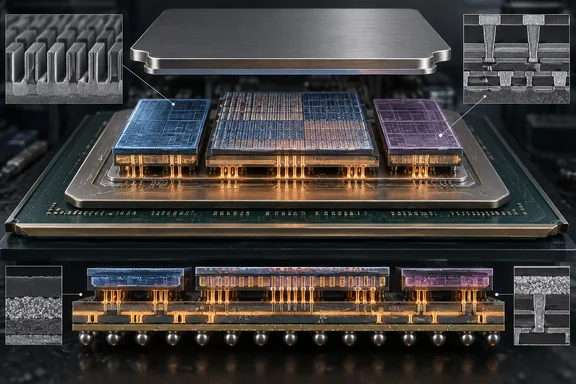
Panther Lake isn't one 18A die. According to SemiAnalysis, it is three active tiles (compute, GPU and I/O) sitting side by side on a passive base tile, connected with Intel's Foveros-S packaging. The mix of processes looks like this:
| Tile | Variants | Process |
|---|---|---|
| Compute | Both variants | Intel 18A |
| GPU (GT1) | 4 Xe3 cores | Intel 3 |
| GPU (GT2) | 12 Xe3 cores | TSMC N3E |
| I/O | Both variants | TSMC N6 |
The practical point is that the top integrated graphics option, the 12-core Arc B390 found in the Core Ultra X9 and X7 parts, is still built by TSMC. Intel's own marketing leans on the "built in the US on 18A" story. TechPowerUp relayed Intel's description of Series 3 as the first AI PC platform built on Intel 18A process technology that was designed and manufactured in the United States. That is true of the compute tile. The graphics and I/O tiles in many configurations come from Taiwan.
SemiAnalysis sees the modular approach as a sensible trade: Intel saves its newest node for CPU logic and uses mature or external processes where they make more sense. The cost is extra bonding, testing, base-die and assembly work.
The teardown also measured one packaging detail. Intel lists Foveros-S bump pitch as nominally 36 micrometres, but SemiAnalysis measured local spacing of about 25 micrometres at one compute-tile edge.
PowerVia: moving the power wiring to the back
In a conventional chip, power and data signals share the same stack of metal layers above the transistors. Power rails take up routing space right where it's most crowded. PowerVia, Intel's backside power delivery, moves the main power network behind the transistor layer. Signals keep the front; power gets the back.
SemiAnalysis's cross-sections show how it works:
- Intel etches narrow "nano-TSVs" (through-silicon vias) from the front, running down from beside each contact into the silicon.
- The frontside signal wiring is completed on top.
- The wafer is bonded to a carrier, flipped over, and the original substrate is ground away until the tips of those buried vias show through.
- Backside copper power layers are built directly onto the exposed vias.
The supply path runs from backside copper rails through molybdenum-lined tungsten nano-TSVs to the transistor contacts. In one cross-section, the tapered connection measured roughly 150 nm from the contact level to the first backside metal layer. The backside stack has fine layers near the transistors and much thicker power wiring closer to the package.
PowerVia also affects cell design. SemiAnalysis says Intel's high-performance libraries shipped with a 36 nm M0 pitch, looser than the 32 nm in the 18A process design kit. Taking the power rails off the signal tracks lets Intel use a compact five-track cell while keeping those wider, lower-resistance wires. The Intel 3 and N3E cells SemiAnalysis measured point to seven-track libraries.
The thermal caveat SSBCrack skipped
SSBCrack says backside power improves thermal management. The teardown describes something more complicated. Because of the backside process, Intel replaces the silicon under its dense logic with dielectric. That cuts parasitic leakage paths and substrate capacitance. It also, in SemiAnalysis's words, "weakens the direct thermal path through silicon," so the contacts, metal layers and package matter more for pulling heat out. The bonded silicon carrier stays on the finished chip and is part of the heat path.
Two more qualifications:
- PowerVia's lateral via landing still uses space inside each standard cell, so it recovers less area than a true direct-backside-contact design would.
- Extra films such as aluminium-oxide etch stops add processing steps, interfaces to manage, and some parasitic capacitance.
Section summary: PowerVia clears congestion from the signal wiring and shortens the power path. It is not a free thermal win, and it doesn't reclaim all the cell area.
RibbonFET: four ribbons, and why that isn't a scoreboard
RibbonFET is Intel's name for its gate-all-around (GAA) transistor. A FinFET's gate wraps a vertical fin on three sides. 18A instead stacks four horizontal silicon nanosheets and wraps the gate completely around each one. The tighter grip on the channel limits leakage as dimensions shrink.
GAA also gives designers a new option. With FinFETs, channel width only changes in whole-fin steps. With nanosheets, width can be adjusted continuously within the design rules: wider sheets for more drive current, narrower sheets for lower capacitance. SemiAnalysis found Intel varying ribbon widths across logic, SRAM and the DDR memory interface.
SemiAnalysis compared the ribbons with Samsung's SF2 process, using an Exynos 2600. Intel has four sheets and Samsung has three. The teardown warns against reading that as a win for Intel. Samsung's sheets are much wider in the areas examined, and sheet width, thickness, polarity and design targets all affect the result. Other differences:
- Gate stack: Intel uses a TiAl-based work-function metal for NMOS and TiN for PMOS, around a hafnium-oxide high-k dielectric, with lanthanum dipoles to tune threshold voltage. SemiAnalysis says that tuning is especially useful because four tightly stacked ribbons leave little room between sheets for thicker metal.
- Contacts: Intel keeps raised source/drain epitaxy under its contacts, which preserves strain, especially for PMOS. Samsung recesses tungsten deep into the epi to cut contact resistance.
These are materials observations from cross-sections. They are not performance benchmarks.
The density verdict: good, not category-leading
This is the finding most likely to annoy the "Intel is back on top" crowd. Using a representative-cell model, SemiAnalysis found Panther Lake's 18A compute logic roughly as dense as the TSMC N3E logic in the same package's GPU tile, and 18.6% denser than the Intel 3 GPU logic it measured. Gate pitches were nearly identical across all three, so cell height accounts for most of the difference.
SemiAnalysis also concludes that 18A does not lead TSMC N3P, N2 or Samsung SF2 in peak density. It notes that whole-die density depends on cell mix and placement, so representative-cell numbers shouldn't be stretched into claims about chip size or speed.
That undercuts some of the January hype. A syndicated FinancialContent piece claimed that by successfully deploying 18A, RibbonFET, and PowerVia, Intel has reclaimed a leadership position in semiconductor manufacturing. The teardown supports a narrower claim. Intel has shipped both GAA transistors and backside power in a volume product. On raw logic density it is competitive, not ahead.
Inside the compute tile: familiar layout, smarter packing
SemiAnalysis says Panther Lake-U closely follows Lunar Lake's floorplan: four P-cores, four low-power E-cores, an NPU, and media and display engines in similar positions. The measured changes:
- Cougar Cove P-cores: about the same area as Lunar Lake's Lion Cove, but with L2 cache up from 2.5 MiB to 3 MiB, which is 20% more L2 in the same space.
- Shared L3: down 14.8%.
- No separate SoC tile: unlike Meteor Lake and Arrow Lake, the NPU, LP E-cores, memory controllers, PHYs and media/display engines all sit on the compute tile, so CPU memory traffic stays on one die. The catch is that analog and I/O circuits now occupy expensive 18A area, and they don't shrink like digital logic. The GPU is still a separate tile and has to cross a die-to-die link to reach DRAM.
- NPU 5: 36.9% smaller than Lunar Lake's NPU 4, with the same total INT8 multiply-accumulate count packed into three larger engines instead of six. It adds native FP8. Scratchpads and SHAVE DSPs were cut from 12 to 6, which SemiAnalysis says may force smaller working tiles or more data movement when AI layers don't fit in local memory.
That matches independent reporting from launch. ITdaily observed that all chips have an NPU on board that is not much more powerful than the NPU of the previous generation. The teardown shows Intel spent the NPU's generational change on area efficiency, not peak throughput.
What this means for Windows laptop buyers and IT fleets
This is my analysis, based on the teardown and general industry knowledge rather than new testing:
- A teardown won't settle battery life or speed. It shows how a chip is built, not how a particular laptop performs. Judge Panther Lake machines on independent reviews of the exact model, since cooling design matters more now that heat has to leave through the metal layers and package.
- Check which GPU tile you're getting. X9/X7 models carry the 12-core TSMC-built Arc B390. Many other SKUs use the 4-core Intel 3 tile. For graphics-heavy users, that difference matters far more than any 18A branding.
- Local AI teams should test FP8. Developers targeting Windows NPU workloads get native FP8 but less on-chip scratchpad. Models need validating, not just recompiling.
- Watch Intel Foundry's roadmap. The teardown shows 18A is real and shipping. Whether Intel can close the density gap with TSMC N2 is the question hanging over its foundry ambitions.
SemiAnalysis says a future newsletter will compare Xe3 across Intel 3, TSMC N3E and Intel 18A, the last of which appears in Wildcat Lake. That should be a cleaner test of what Intel's node can do.
Bottom line: Panther Lake is a real manufacturing milestone, with GAA and backside power in volume consumer silicon. It is not the clean process-leadership win the headlines suggest. The teardown gives Windows buyers a more precise picture of the chip than either Intel's marketing or SSBCrack's premature "launch" story.
References
- Intel Launches Panther Lake Featuring Groundbreaking Backside Power Delivery and GAA Transistors - SSBCrack SSBCrack · 2026-09-27T00:41:59+00:00
- CES 2026: Intel launches 18A 'Panther Lake' Core Ultra 3 ... kitguru.net
- Intel Launches Core Ultra Series 3 "Panther Lake" Mobile Processors on Intel 18A Node | TechPowerUp techpowerup.com