Windows 7 DX11 Cards

Was the wait worth it? Will you be buying one?

  • Price is too high so no to Fermi..

    Votes: 2 16.7%
  • I bought a 5000 series and am happy..

    Votes: 5 41.7%
  • Both Fermi and 5000 series way too expensive

    Votes: 0 0.0%
  • At last! Can't wait to get my Fermi.

    Votes: 0 0.0%
  • I'm waiting until the price drops.

    Votes: 4 33.3%
  • I'm going to wait for the refresh and 512 cores

    Votes: 1 8.3%

  • Total voters
    12
Indeed, I'm surprised the Nvidia chaps didn't start sounding alarms when the 295 shown as inferior to the 260, basically it's invalidated the whole point of a benchmarks job... to show accurate impartial results, without hobbling of any brand or configuration.
 
Southern Islands codenames leaked in Catalyst 10.8

ATI’s latest Catalyst iteration has spilled the beans on a bunch of new Southern Islands codenames and there are a few interesting developments.

A total of 35 new cards were listed in the atiicdxx.da_ file, but sadly we’re still no closer to some actual specs. We already reported the codenames several weeks back, but now we know quite a bit more about the new lineup.

It appears that there are 11 Cayman cards to look forward to and these babies will probably be the most interesting of the lot. Cayman should replace the highly successful HD 5800 series and with a total of 4 different chips and 11 SKUs it appears that ATI has high hopes for it. However, don’t expect a bunch of Cayman-base consumer products, as it appears that 9 of them are reserved for the professional market. Two Antilles dual-GPU cards were also listed and they should be considered part of the Cayman family.

Blackomb and Barts should appear in four iterations each. Barts should replace the Juniper core and it will also be available a professional card, but we’re not sure where Blackomb fits in. Also, two Blackomb parts feature the “Gemini” moniker and frankly we don’t know what to make of it. It seems unlikely that these are dual-GPU cards, although it would be the most obvious conclusion.

Barts is followed by four Whistler cards and three cards based on the Turks core which should replace Redwoon HD 5600 cards. One of the Turk-based cards is codenamed Onega. Seymour (Skinner) also comes in four iterations, two of which are “Gemini” cards. Last in line, three Caicos based cards, one of which is codenamed Caspian. These babies should replace the Cedar HD 5400 core.

It’s quite clear that AMD has its work cut out and Nvidia has quite a few reasons to be worried. AMD seems bent on penetrating the professional market with several Cayman products. As you probably know, the professional market has been Nvidia’s cash cow for years and it’s one of its biggest money makers. However, it’s worth noting that the leak has left quite a few unanswered questions and we will try to find out a bit more soon.

Here's the complete list:

223,CAYMAN GL XT (6700),NI CAYMAN
224,CAYMAN GL XT (6701),NI CAYMAN
225,CAYMAN GL XT (6702),NI CAYMAN
226,CAYMAN GL XT (6703),NI CAYMAN
227,CAYMAN GL PRO (6704),NI CAYMAN
228,CAYMAN GL PRO (6705),NI CAYMAN
229,CAYMAN GL (6706),NI CAYMAN
230,CAYMAN GL LE (6707),NI CAYMAN
231,CAYMAN GL (6708),NI CAYMAN
232,CAYMAN GL (6709),NI CAYMAN
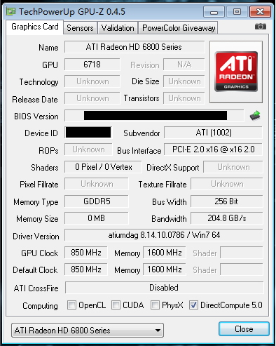
233,CAYMAN XT (6718),NI CAYMAN
234,CAYMAN PRO (6719),NI CAYMAN
235,ANTILLES PRO (671C),NI CAYMAN
236,ANTILLES XT (671D),NI CAYMAN
237,BLACKCOMB XT/PRO (6720),NI BLACKCOMB
238,BLACKCOMB LP (6721),NI BLACKCOMB
239,BLACKCOMB XT/PRO Gemini (6724),NI BLACKCOMB
240,BLACKCOMB LP Gemini (6725),NI BLACKCOMB
241,BARTS GL XT (6728),NI BARTS
242,BARTS GL PRO (6729),NI BARTS
243,BARTS XT (6738),NI BARTS
244,BARTS PRO (6739),NI BARTS
245,WHISTLER XT (6740),NI WHISTLER
246,WHISTLER PRO/LP (6741),NI WHISTLER
247,WHISTLER XT/PRO Gemini (6744),NI WHISTLER
248,WHISTLER LP Gemini (6745),NI WHISTLER
249,ONEGA (6750),NI TURKS
250,TURKS XT (6758),NI TURKS
251,TURKS PRO (6759),NI TURKS
252,SEYMOUR XT/PRO (6760),NI SEYMOUR
253,SEYMOUR LP (6761),NI SEYMOUR
254,SEYMOUR XT/PRO Gemini (6764),NI SEYMOUR
255,SEYMOUR LP Gemini (6765),NI SEYMOUR
256,CAICOS GL PRO (6768),NI CAICOS
257,CASPIAN PRO (6770),NI CAICOS
258,CAICOS PRO (6779),NI CAICOS
 
radeonhd6000kodadiep_dh_fx57.jpg


Catalyst 8.10 driver, the Radeon HD 6000 series will be used in new With the second generation graphics chip, revealing new information for the DirectX 11 cards also began to arrive. According to information obtained from reliable sources Radeon HD 6000 series Antilles, Caymen to Barts and the first stage will consist of three different series. Now, AMD's second-generation DirectX 11 cards for you which end Let's look at the table and what the GPU segment for which we have been tabled.

Code Name Bart: Bart code named AMD new graphics chip, the Radeon HD 6000 series will come into the market is expected to be the first representative. ATI Radeon HD 5700 series GPU power to the Juniper is expected to replace the graphics card, the Radeon HD 6700 series can be expected to be launched in October and will power.

Code Name CAymé: AMD Caymen code named new GPU design, the ATI Radeon HD 5800 series GPU is used to replace the Cypress. Will celebrate its first birthday next month, the Cypress GPU, ATI Radeon HD 5830, HD 5850, HD 5870 and HD 5970 models was used in pairs. Expected to be released in November, ATI Radeon HD 6800 series GPU to be used in designing the Caymen, according to Catalyst 8.10 drivers will be 14 different versions of a significant portion of which will be used in more professional card.

Code Antilles Name: AMD ATI Radeon HD 5970 model, the high-performance year will be updated before the end. According to information received to replace the Radeon HD 6970 Radeon HD 5970'in Antilles model will carry the code name and will have dual GPU Caymen. Radeon HD 5970 Radeon HD 4850 X2 model, unlike models such as X2 and HD 4870 version is expected to double the graphics card is expected in December.

Translated from: Link Removed - Invalid URL
 
Jumping the gun a bit, Microsoft has published on its Windows Update site a new, WHQL-certified Nvidia graphics driver - version 259.47, which features mentions of quite a few unannounced and unreleased desktop and mobile GeForce 400 series cards.

The 259.47 driver is dated August 21st and has support for GeForce 6, 7, 8, 9, 100, 200, 300 and 400 series models, including the following:

- NVIDIA_DEV.0E23.01 = "NVIDIA GeForce GTS 455 "

- NVIDIA_DEV.0DC4.01 = "NVIDIA GeForce GTS 450 "

- NVIDIA_DEV.0DC5.01 = "NVIDIA GeForce GTS 450 "

- NVIDIA_DEV.0DC0.01 = "NVIDIA GeForce GT 440 "

- NVIDIA_DEV.0DE1.01 = "NVIDIA GeForce GT 430 "

- NVIDIA_DEV.0DE2.01 = "NVIDIA GeForce GT 420 "

- NVIDIA_DEV.0E30.01 = "NVIDIA GeForce GTX 470M "

- NVIDIA_DEV.0DD1.01 = "NVIDIA GeForce GTX 460M "

- NVIDIA_DEV.0DD2.01 = "NVIDIA GeForce GT 445M "

- NVIDIA_DEV.0DD3.01 = "NVIDIA GeForce GT 435M "

- NVIDIA_DEV.0DF2.01 = "NVIDIA GeForce GT 435M "

- NVIDIA_DEV.0DF0.01 = "NVIDIA GeForce GT 425M "

- NVIDIA_DEV.0DF3.01 = "NVIDIA GeForce GT 420M "

- NVIDIA_DEV.0DF1.01 = "NVIDIA GeForce GT 420M "

- NVIDIA_DEV.0DEE.01 = "NVIDIA GeForce GT 415M "

The GF106-based GeForce GTS 450 has already been extensively rumored and is said to have 192 CUDA Cores, 1GB of GDDR5 VRAM (128-bit interface), and GPU and memory clocks of 783 MHz and 3608 MHz, respectively. The GTX 460M has also been mentioned in the configuration of a few notebooks but its specs weren't revealed. At least these two are expected in September.

Ref: New GeForce 400 series cards exposed by 259.47 driver | TechConnect Magazine
 
Link Removed due to 404 Error


nvidia.gif


925MHz on a budget


Judging by some early listings, it appears that Nvidia AIBs will offer overclocked GTS 450 cards right from the launch and the pricing looks quite tempting.

A few days ago we wrote about Asus’ GTS 450 DirectCU, but it as it turns out Asus is also preparing an overclocked version with the TOP moniker. According to some GPU-Z screens posted at xtremesystems the board should end up with 925/1850/4000MHz clocks instead of 783/1566/3600MHz. The board was even benched and it managed to match HD 5770 performance in some tests. However, reference boards will end up somewhat slower and isn't on a par with the HD 5770. You can probably expect reference cards to outperform the HD 5750 though and that's what we expected anyway.

Gigabyte is also readying two flavors, the GV-N450 and GV-N450OC but we are clueless about the clocks. An EVGA board, designated 01G-P3-1450-TR, is listed in Australia and New Zealand, but it appears to be reference clocked and it's priced at AUD 177.

However, both judging by several listings in Canada, the overclocked boards should end up less than C$10 more expensive than regular models.

Reference boards are priced between C$149 and C$153, whereas the overclocked boards should sell between C$158 and C$164. For comparison, the same retailers are selling GTX 460 boards for anywhere from C$230 to C$260. All in all the pricing seems quite reasonable, as AMD’s HD 5750 is selling in the C$150 to C$165 price range.

It appears that the GTS 450 could offer good value for money and it should be able to hold its own against 5700 series Radeons in terms of performance. However, it also consumes quite a bit more juice than the Radeons, but at this point it seems like a pretty nice and rather affordable alternative. In any case AMD will introduce the 6000 series within months, so the GTS 450 probably won't be as competitive in the long run.


More...


Link Removed due to 404 Error


Link Removed due to 404 Error


Link Removed due to 404 Error


Link Removed due to 404 Error


Link Removed due to 404 Error

225MHz overclock Nvidia AIB partner Colorful seems to be taking overclocking rather seriously. The outfit has introduced a 900MHz GTX 460 card and it appears to be the fastest 460 around.

The reference clock is 675MHz, so it turns out Colorful managed to overclock it by 33 percent, which is nothing short of impressive. Shader clocks were bumped up to 1800MHz and memory runs at 4200MHz effective.

In order to reach such clocks, Colorful used a new PCB with a 6+1 phase power design rather than the reference 3+1.

The card uses a sizable dual-fan cooler and it doesn’t appear to be too loud, either.
 
Link Removed due to 404 Error


radeon_logo_new.jpg


We've repeatedly heard that the architectural changes in Radeon 6000 generation are not great, but this doesn’t mean that the chip won’t get significantly faster.

This is AMD’s plan. They killed the ATI brand as they want to move towards Fusion, CPU meats the GPU design, but as you can see Radeon sticks for discrete graphics of the future.

The new Radeon HD 6000 is a tweak to an existing architecture that will squeeze better performance per watt, better performance overall and some new things like UVD 3.0 that will make better use of six Display ports and make it more affordable to actually use such a setup.

Naturally decoding and encoding will get faster and better, but it was already quite good. The chip is an evolution rather than a revolution and the real revolution comes in 28nm, at some point in 2011 and no, the revolution will not be televised.

We've already have reported that the new cards should start showing up as of October, with a dual-GPU card comming before the end of the year and the first leaked benchmarks are showing that the Radeon HD 6000 has a lot of potential.
 
Link Removed due to 404 Error


Link Removed due to 404 Error


Might make sense

According to a post over at Donanimhaber.com, AMD's upcoming Radeon HD 6700 series might have a 256-bit memory interface.

The 256-bit memory interface comes as a surprise considering that the current HD 5700 series features a 128-bit memory interface, but it could make sense as all reports indicate that the upcoming HD 6000 series graphics cards are all about evolution.

This also could be the way to keep the available HD 5700 series alive as AMD can drop its price and keep selling it until they clear out the stock as thanks to the "evolution" and the wider memory interface, HD 6700 series should end up significantly faster.

Judging by some early benchmarks, HD 6000 cards will offer a significant performance boost over the current generation, but bear in mind that they still stick to the same 40nm production process. Using a wider memory bus could be one of the ways of boosting performance while using the same production process, but it would also increase production costs.
 
Last edited:
The guys from Chiphell.com managed to score what is claimed to be a working prototype of AMD's Radeon HD 6000 Series graphics card codenamed "Cayman XT." According to the info, the pixellized card is the XT version of the Cayman chip and should be the Radeon HD 6x70 series card, at least if AMD sticks to the rumoured naming scheme.

Unfortunately, the picture doesn't reveal much solid information rather than some speculaction that the card might be as long as the Radeon HD 5870, should have CrossFireX support, and has two DVI ports, an HDMI port and two mini-DisplayPort connectors. The post didn't reveal any other specifications, except that we are looking at a GPU made on TSMC's 40nm manufacturing process.

An interesting detail is that the prototype still proudly carries the ATI brand sticker, something that AMD will probably throw away soon enough. In any case, it looks like more info regarding AMD's Radeon HD 6000 Series family has finally started to trickle out, which means that we'll see more surface very soon.

AMD_Caymanpix_1.jpg


Ref: Link Removed due to 404 Error
 
Link Removed due to 404 Error

nvidia.gif
geforce_400m_logo.jpg


Top to bottom solutions based on GF104, GF106, GF108

Over the past several months, a significant portion of the mobile DirectX 11 market has been predominated by AMD Radeon Mobility 5000 Series parts. The red team has enjoyed a fair share of design wins, and one of the highest selling points can be attributed to the DirectX 11 feature itself. Nevertheless, the time has arrived for Nvidia to respond with a slew of second-generation mobile Fermi parts catered for a variety of high-end, performance and mainstream budgets.Back in May, Nvidia launched its flagship Geforce GTX 480M for gamers and mobile enthusiast customers. What surprised most of the industry was the fact that the company had actually used a full GF100 chip which featured the same number of cores as the desktop Geforce GTX 465. Mobile power constraints were tight and exceptionally high, as the GPU consumed 100W alone. Nevertheless, the company has indicated that it intends to capitalize on Optimus Technology as a means to dynamically distribute power between an IGP-enabled GPU and its discreet GPUs.

High-end GPUs: Geforce GTX 480M, Geforce GTX 470M, Geforce GTX 460M
Today, the company has added the Geforce GTX 470M and Geforce GTX 460M to its high-end mobile DirectX 11 offering, which only included the Geforce GTX 480M up until this point. The Geforce GTX 470M features a 535MHz core clock, 288 CUDA cores operating at 1100MHz, and a 192-bit GDDR5 memory interface operating at 1250MHz with 60GB/s memory bandwidth. This GPU replaces the Geforce GTX 260M with 55W TDP and should fit in a similar power envelope. As AnandTech noted, the core count between generations raises from 112 at 1375MHz to 288 at 1250MHz, an increase of 134 percent. The chip should theoretically double computational performance over its predecessor. However, the memory bandwidth of both GTX 260M and GTX 470M is 60GB/s, and it will be interesting to observe if Nvidia's decision to leave memory bandwidth the same may have any effects on gaming performance.
geforce_gtx_470m.png

In addition, the Geforce GTX 460M features a 675MHz core clock, 192 CUDA cores operating at 1350MHz, and a 192-bit GDDR5 memory interface operating at 1250MHz with 60GB/s memory bandwidth. This GPU replaces both the Geforce GTS 360M and Geforce GTS 350M, neither of which made a significant presence in the notebook market. The chip should also fit in a similar power 40W TDP envelope. Just like the GTX 470M, the chip should theoretically double computational performance over its predecessors, and the memory bandwidth story is the same as the GTX 470M.

Performance and Mainstream GPUs: Geforce GT 445M, Geforce GT 435M, Geforce GT 425M, Geforce GT 420M, Geforce GT 415M
When AMD launched its performance and midrange Radeon Mobility HD 5000 Series GPUs, many analysts noted that performance drops between the high-end segment and the midrange segment were rather significant. For instance, the drop from Radeon Mobility HD 5800 Series to the HD 5700 and HD 5600 parts often expressed less than half the computational performance. Meanwhile, the majority of consumers in this market range weren't too concerned, as long as the associated notebook device combined the "DirectX 11" logo with a reasonable TDP envelope and ensured strong battery life for day-to-day productivity purposes.
Now that Nvidia's engineers have spent a considerable amount of time refining transistor leakage, high amperage choices and other hardware problems that plagued the original GF100, the company is ready to release much cooler mobile versions of its second-generation chips, GF104, GF106 and GF108. From top to bottom, Nvidia's performance to midrange mobile GPU segment includes the Geforce GT 445M, Geforce GT 435M, Geforce GT 425M, Geforce GT 420M and Geforce GT 415M. From the start, none of these GPUs support SLI, as the company has reserved the feature for its high-end market.
The Geforce GT 445M is the only GPU that can be a mixed bag in terms of hardware specifications. It features a 590MHz core clock and 144 CUDA cores at 1180MHz. However, memory configurations will be available in both a 128-bit DDR3 memory interface operating at 800MHz with 25.6GB/s bandwidth, or a 192-bit GDDR5 memory interface operating at 1250MHz with 60GB/s bandwidth. As AnandTech notes, it appears that the Geforce GT 445M will use the GF104 chip for the higher bandwidth model and GF106 for the lower bandwidth model. In terms of computational performance, the GPU is equivalent to roughly two-thirds of the higher end Geforce GTX 460M for the higher bandwidth 192-bit GDDR5 model. At this point, we are unsure of the extent in which the different bandwidth rates will effect gaming performance, but it would be safe to double check GPU specifications before purchasing a new notebook with a GT 445M.
geforce_gt_445m.png

From here on down, the rest of Nvidia's performance and mainstream GPUs use DDR3 memory interfaces. The Geforce GT 435M features a 650MHz core clock, 96 CUDA cores operating at 1300MHz, and 128-bit DDR3 operating at 800MHz with 25.6GB/s memory bandwidth. This GPU directly replaces the Geforce GT 335M, which was famously popularized by the Alienware M11x ultraportable gaming notebook. The core count between generations raises from 72 at 1080MHz to 96 a 1300MHz, but memory bandwidth decreases from 34.1GB/s to 25.6GB/s. In terms of computational performance, the GPU should have a significant 60 percent performance advantage over its predecessor within the same TDP envelope. Based on these numbers alone, we are inclined to believe that Alienware is already at work on a refresh of the M11x, but this time with DirectX 11 and more architectural horsepower.
geforce_gt_435m.png

The Geforce GT 425M features a 560MHz core clock, 96 CUDA cores operating at 1120MHz, and 128-bit DDR3 operating at 800MHz with 25.6GB/s memory bandwidth. This GPU directly replaces the Geforce GT 325M and should be based on GF106. The core count between generations doubles from 48 at 990MHz to 96 at 1120MHz, but both feature the same memory bandwidth. In terms of computational performance, the GPU should have roughly a 35 percent performance advantage over its predecessor despite having the same amount of memory bandwidth.
In similarity, the Geforce GT 420M features a slightly reduced 500MHz core clock, 96 CUDA cores operating at 1000MHz, and 128-bit DDR3 operating at 800MHz with 25.6GB/s memory bandwidth. This GPU also replaces the Geforce GT 325M and should also be based on GF106.
geforce_gt_425m.png

At the bottom of Nvidia's mainstream mobile DirectX 11 list is the Geforce GT 415. Rest assured, the chip packs more punch than many may expect. It features a 500MHz core clock, 48 CUDA cores operating at 1000MHz, and 128-bit DDR3 operating at 800MHz with 25.6GB/s memory bandwidth. This GPU replaces the rather economical Geforce 310M and Geforce 305M and should be based on GF108. What's surprising about the Geforce GT 415 is that the core count literally triples between generations, from 16 at 1150MHz (GT 305M) and 1530MHz (GT 310M) to 48 at 1000MHz. Memory interface width doubles from 64-bit DDR3 to 128-bit DDR3, and memory bandwidth also doubles from 12.8GB/s to 25.6GB/s. With these numbers, even the lowest mobile Fermi-based GPU to launch should see a sizable difference in computational performance.
geforce_gt_415m.png


As several analysts have noted, the Geforce GT 310M is already roughly three times faster than Intel's HD Graphics solution and nearly twice as fast as AMD's Radeon Mobility HD 4200 IGP in the 785G chipset. With more users transcoding HD video content on their notebooks, browsing Google Earth in 3D rather than using Google Maps, and utilizing the GPGPU acceleration features of Photoshop CS5, Mozilla Firefox 4 and Google Chrome 7, even the performance of the Geforce GT 415M should serve as a compelling reason to upgrade to a DirectX 11 capable GPU. Nvidia has finally managed to pull its head back in the game, at least in the mobile space. The company's impact on the midrange, performance and high-end desktop GPU markets in 2010 remains another question entirely. Regardless of the competitive advancements at hand, whether or not the decision is AMD or Nvidia, the consumer always wins in the long run.


Link Removed due to 404 Error


Fastest single-GPU arriving to market
Over the weekend, member Link Removed due to 404 Error of Chinese language forum PCInLife made news by posting the first unconfirmed screenshots of Radeon HD 6800 Series performance benchmarks. In what would normally be considered a baseless rumor without empirical evidence, we found this forum post to contain enough verification to deem it plausible for discussion. Our good friend Lars-Göran Nilsson fromSemiAccurate was able to speak with the creator behind the GPU-Z graphics information utility, who was able to confirm that the screenshots presented below appear to be the real deal.


radeon_6000_series_3dmark_vantage_1.jpg


Radeon HD 6800 Series (Cayman XT) 3DMark Vantage Extreme Test 1


radeon_6000_series_3dmark_vantage_2.jpg


Radeon HD 6800 Series (Cayman XT) 3DMark Vantage Extreme Test 2

radeon_6000_series_3dmark_vantage_3.jpg


Radeon HD 6800 Series (Cayman XT) 3DMark Vantage Performance Test 3

WG_Baby did not provide any system specifications associated with the 3DMark Vantage Extreme overall score. However, several analysts concur that an Intel Core i7 processor must have been used as a result of the high CPU subscore. Nevertheless, if the GPU managed to subscore X11634 on the first run, X11762 on the second run and P24056 on the third run with default clocks, this would seem to indicate that Cayman XT may become the fastest single-GPU card to launch on the market. The only exception in its path would be the Radeon HD 5970 dual-GPU, which will eventually be succeeded by Antilles XT.


radeon_6000_series_gpu-z.png


The accompanying GPU-Z 0.4.5 information reveals "6718" as the GPU ID, along with an 850MHz core clock and 1600MHz memory clock comprised of 256-bit GDDR5 with 204.8GB/s memory bandwidth. According to the Link Removed due to 404 Error last week, the GPU ID matches as "233, Cayman XT (6718) NI."
As VR-Zone mentioned last Thursday, many of the codenames for AMD's next generation Radeon cards refer to West Indies islands located in the Carribbean. Based on their respective geographic regions, theGreater Antilles region of the West Indies comprises the Cayman Islands because of their geographical proximity to Cuba. In contrast, the Lesser Antilles region comprises St. Barts, Turks Caicos, and Seymour islands. If we can accurately map these anecdotal references into AMD's codename strategy, we can logically infer that Cayman GL XT, Cayman GL Pro, Cayman GL, Cayman GL LE, Cayman XT, Cayman Pro, Antilles Pro and Antilles XT all belong to the Northern Islands GPU family. Nevertheless, the codename mixup between Southern Islands and Northern Islands graphics card families remains inconclusive for now.


We are also aware of the fact that the "ATI" brand name appears in the GPU-Z Name information box, despite AMD's intentions to retire the brand later this year in order to make way for its Fusion marketing agenda. Although this reference may be attributed to the way GPU-Z has been programmed, perhaps this next-generation consumer desktop GPU family will become the last to feature the proud "ATI Radeon HD 6000 Series" title before DAAMIT tosses "ATI" from its brand image entirely. The outcome remains in question until more information behind the company's Q4 launch schedule is revealed.


Update: In addition to the obligatory 3DMark Vantage tests, WG_Baby recently updated his findings to include Crysis (2007) and Unigine Heaven 2.1 benchmarks. The results show that the Cayman XT graphics card and currently unknown hardware combination can render the original Crysis at an overall average 43.55 frames per second on Very High settings at 1920x1200 with 4x AA in DirectX 10 64-bit mode (which shouldn't have been used, as Crysis 64-bit mode is known to lower framerates by an average of 5fps with no performance advantages over 32-bit mode).


radeon_6000_series_crysis_benchmark.jpg


Additionally, the Unigine Heaven 2.1 benchmark test was run at 1920x1200 fullscreen resolution with 4x AA, 16x AF and Extreme Tessellation enabled. The results show that the Cayman XT gets 922 Scores with an average 36.6 frames per second.


radeon_6000_series_unigine_benchmark.jpg


Upcoming Radeon HD 6000 Series Is All-New Architecture

AMD originally wanted a brand-new architecture (the first since Radeon HD 2000 series) on TSMC's 32-nm node, and it was codenamed "Northern Islands." Then they hit a snag: TSMC cancelled their 32-nm, instead deciding to go straight to 28-nm in 2011. At this point, a new family codename called "Souther Islands" came about; apparently it was still 40-nm, and would be a more efficient version of "Evergreen" (Radeon HD 5000 series).

This is not true. The upcoming Radeon HD 6000 series IS "Northern Islands" and IS a brand-new architecture. After the 32-nm process was cancelled, AMD moved "Northern Islands" back to the 40-nm node (obviously it probably lost a few shader/texture/pixel units to what AMD had planned for 32-nm), and also started work on "Southern Islands." The "Southern Islands" family will be a 28-nm die-shrink of "Northern Islands" and will most likely be manufactured at Globalfoundries (though it could still be TSMC, or even both).

The end point to take away is that the Radeon HD 6000 series is a new architecture, and that more than helps explains some of these insane early benchmarks that have been floating around. Die sizes are said to be about 10-15% bigger across the board, but the performance also looks to be 60%+ higher in some cases; more than a fair tradeoff. It's time to get excited for new GPUs again.

Ref: Upcoming Radeon HD 6000 Series Is All-New Architecture | VR-Zone | Gadgets | PC Enthusiasts
 
256-bit memory interface

Right after Cayman and Caicos prototype pictures surfaced, the guys from ChipHell Forums also posted a picture of a prototype Barts XT card, which should end up designated as Radeon HD 6770 unless AMD decides to change its naming scheme at the last minute.

Bear in mind that we are still looking at prototype cards and that the actual retail samples might end up to be a bit different as we are pretty sure that it won't show up in the market with the pixellized cooler. Although the specs are still unknown, it can be seen from pictures that the card need two 6-pin PCI-Express power connectors, has singe Crossfire connector and has two DVI, an HDMI and two mini-DisplayPort connectors.

The card should have a 256-bit memory interface and, according to rumours, an 80% to 100% increase in memory bandwidth when compared to the previous generation.

amd_barts_1.jpg


amd_barts_2.jpg


Ref: Link Removed due to 404 Error
 
Link Removed due to 404 Error


gainward_logo.gif


Goes Like Hell at 930MHz


Gainward
has decided to roll out no less than three different GTS 450 cards. As expected, all three cards are based on the 40nm GF106 GPU, have 192 CUDA cores and 128-bit memory interface paired up with 1GB of GDDR5 memory.

All three cards feature Gainward's own design and as you can see from the picture below, Gainward's cards feature two DVI, VGA and HDMI outputs. The reference and the Golden Sample card will use BCBG Fan-Sink cooler while the Goes Like Hell version will be able to brag with GP Heatpipes cooler with 6mm copper heatpipes and copper base.

The reference card works at 783MHz for the GPU, 1566MHz for CUDA cores and 3608MHz for memory while the Golden Sample version got overclocked to 880MHz for the GPU, 1760MHz for CUDA cores and 3900MHz for 1GB of GDDR5 memory. The cream of the crop is the Gainward GTS 450 1GB Golden Sample - Goes Like Hell card that got overclocked to an impressive 930MHz for the GPU, 1860MHz for those 192 CUDA cores and 4000MHz for the same 1GB of GDDR5 memory.

All three cards are listed at Link Removed - Invalid URL with price set at €122,90 for the reference card, €127 for the Golden Sample card and €139,90 for the Goes Like Hell edition.

gainward_GTS460GLH_1.jpg


gainward_GTS460GLH_2.jpg


Link Removed due to 404 Error


tgtpov_logo.jpg


Ultra Charged with Triple Fan Cooling

Point of View and TGT Tuning have rolled out its latest addition to the GTX 400 series, the POV/TGT Geforce GTX 480 Ultra Charged Triple-Fan-Cooling. This triple-slot behemoth is factory overclocked to 763MHz for the GPU and features Arctic Cooling's Accelero Xtreme Plus cooler in order to be as silent as posible.

POV/TGT GTX 480 Ultra Charged works at 763MHz for the core, 1526MHz for shaders and 3800MHz for 1536MB of GDDR5 memory. Note that the card only has a 3MHz higher clock than the regular POV/TGT GTX 480 Ultra Charged, but in turn should be much cooler and most importantly a lot more quieter.

The triple-slot, triple-fan cooler features a total of five heatpipes and 84 fins combined with copper block and three ultra quiet 92mm PWM fans with low noise impeller.

The new POV/TGT "Made in Germany" GTX 480 UltraCharged TFC card should be available in retail/e-tail as of September 20th.

povtgt_GTX480UCTFC_1.jpg


Link Removed due to 404 Error


radeon_logo_new.jpg


256-bit bus, 960 shaders

Chinese tech site Chiphell has leaked an interesting slide featuring full AMD Barts specs and the numbers look impressive.

The new Barts series should succeed Juniper-based HD 5770 and HD 5750 boards, but it will deliver a significant performance boost. The biggest difference is the transition to a 256-bit memory bus, which will provide quite a bit more bandwidth than the 128-bit Juniper series. Both boards should feature 1GB of memory, but we’re still not sure about memory clocks, as we’re getting some mixed information.

Barts XT will feature 12 SIMDs, 960 shaders, 48 texture units and 32 ROPs. For comparison, Juniper XT packs 800 shaders and 40 texture units, so Barts will have 20 percent more of everything. The core should end up clocked at 850MHz and the TDP is rated at over 150W, which is quite a bit more than the HD 5770.

Barts PRO packs 800 shaders, 40 texture units and 32 ROPs, much like the current Juniper XT, but it will also have a wider 256-bus. It will be clocked between 700MHz and 725MHz and its TDP should end up below 150W.

AMD is pitting both boards against Nvidia’s GTX 460: Barts PRO will take on the 768MB version of Nvidia’s GTX 460, while Barts XT should fight the 1GB version. Judging by the spec, Barts boards should be able to outperform the GTX 460 and we wouldn't be surprised if they match HD 5830 or even 5850 performance in some scenarios, thanks to higher clocks and the 256-bit bus.

More here.

Link Removed due to 404 Error

 
ATI Radeon HD 6800, for the first time in our hands
We had the opportunity to literally get your hands on an engineering sample of ATI Radeon HD 6000 family at an event focused on computing GPU and CPU, which AMD has participated with a stand.
The card was taken to be shown to partners and customers, not expecting the presence of persons of Ubuntu that, technically, are not among those who should have access to this product.

The card belongs to the family of products Nothern Island, built with 40 nm process from TSMC solutions like the Radeon HD 5000. Southern Island with the name are indicated next generation of video cards built using 28-nanometer production technology, these products can be envisaged a launch period between late 2011 and early 2012, at least according to the information currently available.

The card codenamed Cayman, then placed in high-end segment of desktop solutions targeted at the most demanding gamers. The official name is currently unknown but is likely to take to Radeon HD 6800, according to the logical framework used by AMD for its desktop video cards made in recent years.

The overall dimensions as the first impression seems to be the same as the ATI Radeon HD 5870, with the latter than the reference design does not end at the rear with two openings nicknamed "Batmobile", but is completely enclosed by a plate aluminum black with red stripes. The remainder of the card is completely covered by a plastic shell similar to that adopted for the Radeon HD 5800 series, after the PCB is fully visible, in the absence of surface components.

Just looking at the back of the card we have noted the points of contact for 8 modules GDDR5 memory, which is then confirmed using a 256bit memory bus size for this card like the 5800 Series solutions. The upper part contains a power connector 6-pin PCI Express flanked by an 8-pin, technical choice identical to that of dual GPU cards ATI Radeon HD 5970, note that the ATI Radeon HD 5800 series are equipped with two connectors PCI Express 6-pin.

We can then estimate, for this card, the GPU is clocked higher than that made available by ATI Radeon HD 5870, with similar dynamics including the GDDR5 memory, which should significantly exceed the 4800 MHz clock effective solutions Radeon HD 5870 on the understanding the magnitude of the bus.

The rear panel connections sees the presence of two DVI ports, a standard HDMI and two mini-display port, a configuration like this without imagining that it is possible with this type of card, configure the technology Eyefinity up to a maximum of 4 screens used simultaneously.

Unfortunately we do not have detailed information on what's new AMD architecture implemented within these new generations of GPUs, we can also confirm whether there has been a radical change in the structure of stream processors than the solutions chosen for the family R800, although it had the feeling that with this generation of GPUs AMD has taken so important to review your architecture, with the limited data using 40-nanometer manufacturing technology with which these GPUs will be built.

We chose not to publish pictures of this card, to protect our source but we can confirm that the card is ready and that the debut would be a matter of no time.
Ref: ATI Radeon HD 6800, per la prima volta tra le nostre mani - Hardware Upgrade - Il sito italiano sulla tecnologia - www.hwupgrade.it
 
Nvidia details performance improvements of new GPU architectures

During the GPU Technology Conference, Nvidia CEO Jen-Hsun Huang surprised hardware journalists with a very surprising announcement regarding the lineup of next-generation Nvidia GPU architectures.
"For the very first time in the history of our company, we are going to tell you the codenames and the direction of our next several generations of processors," said Jen-Hsun Huang. We’re shipping Fermi today, which brought to the world very high-performance double precision. Fermi is rated at 768GFLOPS peak."
Jen-Hsun presented a keynote slide to the audience revealing two upcoming GPU architecture codenames, Kepler 28nm (2011) and Maxwell (2013).
"Our next-generation GPU, Kepler, also named after a scientist, is expected to deliver 3-4x the performance-per-watt of Fermi. Kepler is based on 28nm and we expect to go into production next year. By the time that we’re done with the Kepler family, we wil have probably invested a couple billion dollars in R&D for it. Kepler will achieve a big step up in comparison to Fermi in the area of performance-per-watt”
Jen-Hsun went on to explain the major design problem that faces parallel computing architectures. In perspective - "transistors are free, but power is not. If we are conscious about the use of performance-per-watt architectural ideas, then we'll continue to expand performance along with the number of transistors in new architectures."
Nvidia's CEO continued by announcing Maxwell, an even more futuristic architecture expected to be delivered in 2013. "Maxwell is going to be 16x performance improvement relative to our last GTC (2009). In just a few more years, we’re going to see a 16x improvement in performance for parallel computing applications. Between now and Maxwell, we’re going to introduce features like virtual memory. We’re going to enhance the GPU’s ability to autonomously process, so it’s less dependent on the CPU, along with a very large improvement in performance.”

Ref: Link Removed due to 404 Error
 
Nvidia Maxwell is 22nm part

40 times faster than Fermi


In 2013 Nvidia plans to launch a Maxwell chip and Jensen just told at the press conference that the new chip is 40 times faster than Fermi and that it will get up to 10 to twelve times faster than Kepler.

The manufacturing process of choice is 22nm, something that TSMC hopes to have in 2013 but it still leaves quite a gap in 2012 when there won’t be anything really new, just maybe a tweak in Kepler.

This is a long time to wait for a new architecture, but at the same time it's all about the FABS that simply won’t be ready. 28nm only comes in 2011 and until 2013 we will be stuck with it.

Ref: Link Removed due to 404 Error
 
AMD's 6870 coming in November

Early silicon doing very well

by Charlie Demerjian

September 24, 2010

Link Removed due to 404 ErrorIT LOOKS LIKE ATI's, sorry AMD's, 6870 is on track and doing quite well. Early word from AMD central has two big thumbs up.
We have already told you about the first member of the ATI's, sorry AMD's, Northern Islands family taping out, it is called Barts. Barts is a mid-range part aimed squarely at the Nvidia GF104/GTX460 chip, likely called the HD6770. It is due out really soon and should obliterate the competition.
Cayman, the big brother to Barts, taped out a little over a month after Barts, so it was expected to hit the streets a little after a month from Barts as well. This would put the 6870 on the streets in mid to late November. SemiAccurate's sources tell us that that is exactly what is happening.
Shipments to OEMs are going to start around the same time Barts/6770 hits the street. This puts cards 2-4 weeks out, well in time for Black Friday. Unlike previous Black Friday rumors, this card is real, not a puppy wielding wood screws.
In another turn of events, unlike the last round of cards bearing the last three digits of 870, this round should have very plentiful supply. While there will always be initial shortfalls due to demand, this time around wafer supplies are much higher. To top it off, yields are very good, the first batch of silicon from the fab is yielding far better than 5870/Cypress did at the same stage.
The end result is November should have a plentiful supply of Northern Islands cards, both 67x0 and 68x0s. If demand isn't insane, dual Cayman cards, aka Antilles, should be on the market as 69x0s before the end of 2010. If demand is too high for the 6870, then 6970 may be delayed a bit until there is adequate supply. ATI, sorry AMD, did learn from the last time.
Stick around, the rest of 2010 is going to be very exciting from a GPU standpoint, and early 2011 looks just as good. Unless you are an Nvidia stockholder, then it won't be nearly as fun.S|A

Ref: SemiAccurate :: AMD's 6870 coming in November
 
Back
Top