

KeplerL2 Says Project Helix and PS6 Silicon Have Taped Out
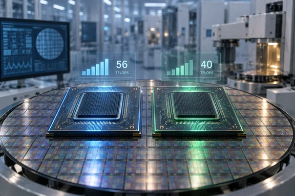
The claim came from a forum exchange, not an announcement. As VideoCardz reports, asked whether the two chips had already taped out, Kepler confirmed both taped out. In the same NeoGAF discussion, Kepler also shared GPU compute estimates of 40 TFLOPS for PS6 and 56 TFLOPS for Xbox Helix.
Other outlets picked up the same forum post within hours. China's GamerSky and Germany's Playfront both ran the tape-out and TFLOPS claims. Those stories repeat one source, KeplerL2, and don't confirm it independently. Playfront adds a detail the others lack. It says that, according to Kepler_L2, Sony's final silicon design is now moving into the physical manufacturing of prototypes at TSMC. No other outlet has reported the foundry detail as part of this leak. Read it as the leaker's claim, not a confirmed manufacturing arrangement.
KeplerL2 has a history on this topic. In February, TechSpot described the leaker as "reliable leaker Kepler_L2" in its coverage of the PS6 specifications, and several of the numbers in circulation now trace back to Kepler's earlier posts. A good track record makes a claim worth reporting. It doesn't make it a spec sheet.
Tape-Out Marks the End of Design Work on the Helix SoC, Not the Start of Production
Tape-out means a chip design has been finalized for submission to manufacturing. The term dates from when chip layouts were literally written to magnetic tape and sent to the fab. Today it means the design team has frozen the layout and handed it to the foundry to make the photomasks used to print the first wafers.
VideoCardz argues that at this stage, major specification changes are generally not expected unless testing uncovers problems that require further silicon revisions, and even then, those revisions typically address hardware bugs rather than change the overall specifications. That's a fair reading of how tape-out usually works. The compute unit count, memory interface and cache sizes are baked into the layout. What can still change is clock speed, which depends on how the physical silicon behaves, and clock speed feeds directly into any TFLOPS figure.
Tape-out doesn't tell you that working chips exist, that validation has passed, or that production has started. Playfront puts it this way: the tape-out marks the end of the pure simulation model phase, and developers are now building physical test chips for post-silicon validation. The same outlet estimates that this stage typically takes 18 to 24 months in the semiconductor industry. That's Playfront's industry rule of thumb, not a schedule from Sony or Microsoft.
For Helix, the one official timeline is Microsoft's developer milestone. At the 2026 GDC Xbox Developer Summit, Xbox's Jason Ronald confirmed that "alpha versions" of Project Helix will start going out to developers in 2027. Actually, that claim comes from VideoCardz's separate GDC coverage, which also noted that the date does not give a retail launch date, but it does place the platform in an early developer phase rather than near release. A tape-out in late 2026 fits that schedule, since alpha dev kits need real silicon. It doesn't turn the 2027 developer date into a retail date.
Why 56 Versus 40 TFLOPS Is a 40% Paper Gap, Not a 40% Frame-Rate Gap
The arithmetic is simple. 56 is 16 more than 40, so Helix is 40% higher. VideoCardz adds the necessary condition: the two estimates put Xbox Helix ahead of PS6 in theoretical GPU compute throughput, assuming both use the same counting method.
A TFLOPS figure (trillions of floating-point operations per second) is a peak number. It multiplies the GPU's shader lanes by the operations each lane can do per clock, then by the clock speed. According to GamerSky, KeplerL2 said in the thread that the figures represent only FMA (fused multiply-add) throughput. Kepler also argued that normalising TFLOPS across different GPU architectures isn't scientific, and noted the same argument broke out over RDNA figures when PS5 launched.
That argument is already running. Earlier this year, when the 40 TFLOPS PS6 figure first appeared, a NeoGAF commenter argued that 54 CUs running at 3 Ghz gives us 20 tflops, and the 40 tflops is inflated numbers AMD has been using since RDNA3. The disagreement is about dual-issue execution. Since RDNA 3, AMD's shader units can, under the right conditions, issue two FP32 instructions per clock, and AMD counts that doubled rate in its peak TFLOPS.
Working the dual-issue math
My own arithmetic shows where both numbers come from. It assumes the widely rumoured 54 compute units for PS6 and standard AMD counting of 64 FP32 lanes per CU and two operations per FMA. At 3 GHz, 54 × 64 × 2 × 3.0 comes to about 20.7 TFLOPS single-issue, or about 41.5 TFLOPS with dual-issue counted. PS5's official 10.28 TFLOPS comes out exactly from 36 CUs at 2.23 GHz using the single-issue formula, without dual-issue.
So the jump from PS5 to PS6 looks like roughly 4× on paper, but part of that is a change in how the number is counted, not extra hardware. Dual-issue only pays off when the compiler can find pairs of independent instructions, so real games get less than the doubled peak. TweakTown has already caught one analysis making this mistake. It found that doubling the 34 - 40 TFLOPS figure again appears to count Dual Issue twice, which produced an inflated 68–80 TFLOPS estimate for PS6.
The Helix-versus-PS6 comparison holds up better. If KeplerL2 counted both chips the same way, as the leaker's stated FMA-throughput definition suggests, the 40% ratio survives the counting problem even though the absolute numbers don't compare to older consoles. VideoCardz also notes that memory bandwidth is quite important in games, and ray-tracing hardware, CPU performance, power limits and developer optimisation all affect real frame rates. A peak FMA figure captures none of these.
The Rumoured Helix Lead Has Grown From Earlier 25% Estimates
The 56 TFLOPS figure changes the story in one way the original report doesn't flag. Earlier leaks had Microsoft's lead as smaller. In March, GamingBolt reported a Moore's Law Is Dead claim that the Magnus chip powering Project Helix is expected to be around 25 percent faster than the PS6 on paper. ("Magnus" is the rumoured codename for the Helix SoC.) KeplerL2 said much the same in a March NeoGAF thread, writing that for Magnus it's ~25% higher TFlops/Tex rate, ~33% higher Front-end BW, Geom rate, Pixel rate plus 140% more LLC and 20% more memory bandwidth.
A 25% gap and a 40% gap don't match. The leak doesn't explain the difference. Possible reasons include different clock targets, a larger GPU configuration than first rumoured, or the earlier figure measuring something slightly different. Any of these is a guess, not a documented fact. If both of Kepler's figures are accurate, Microsoft's paper advantage has grown since spring.
Kepler's March comparison is also the best guide to how much a TFLOPS gap is worth. In that post, Kepler compared the Magnus gap with the current generation, noting that XSX has 20% higher TFlops and Texture Fill rate plus 20% more LLC and memory bandwidth but 18% lower Front-End bandwidth, Geometry rate and Pixel Fill rate. Xbox Series X's 20% compute lead over PS5 did not produce a consistent 20% advantage in multiplatform games. A NeoGAF commenter summed up the lesson in the same threads: "Everyone thought series X will wipe the floor with PS5 until the last moment." The CPU side of the rumour points the same way. GamingBolt reported that Helix's CPU is expected to be more powerful thanks to its inclusion of Zen 6 cores, compared to the PS6's Zen 6c cores, but the difference isn't expected to be too large between the two consoles when it comes to overall performance.
For reference, here are the published current-generation figures next to the rumoured next-generation ones. Xbox Series S is rated at 4 TFLOPS and Series X at approximately 12 TFLOPS, Sony's PS5 reaches 10.28 TFLOPS, while PS5 Pro has a published rating of 16.7 TFLOPS.
| Console | GPU compute | Status |
|---|---|---|
| Xbox Series S | 4 TFLOPS | Shipping |
| Sony PS5 | 10.28 TFLOPS | Shipping |
| Xbox Series X | ~12 TFLOPS | Shipping |
| Sony PS5 Pro | 16.7 TFLOPS | Shipping |
| PlayStation 6 | 40 TFLOPS | Rumoured (KeplerL2) |
| Project Helix | 56 TFLOPS | Rumoured (KeplerL2) |
Given the dual-issue counting change above, the bottom two rows don't compare directly with the top four.
Microsoft's Confirmed Project Helix Features Point Beyond Raw Compute
What Microsoft has actually confirmed about Helix says more about its design goals than any TFLOPS leak. At GDC 2026, Jason Ronald said the system will use a custom AMD chip, support both Xbox and PC games, and deliver what Microsoft described as an order-of-magnitude increase in ray tracing performance, including path tracing. Microsoft's own statement said Helix is powered by a custom AMD SoC and co-designed for the next generation of DirectX and FSR.
The rendering features Microsoft listed are mostly specialised workloads that a peak FP32 figure doesn't measure. VideoCardz reported that the GDC hardware slide listed "AMD FSR Next + Project Helix," next-generation ML upscaling, and a new ML Multi Frame Generation feature. It also named GPU Directed Work Graph Execution, next-gen ray regeneration for ray tracing and path tracing, neural texture compression, deep texture compression, and DirectStorage + Zstd. Machine-learning upscaling and frame generation lean on AI accelerators, and path tracing leans on ray-tracing hardware. VideoCardz makes the same point, noting that TFLOPS do not account for how many Ray Accelerators the chip has.
Sony appears to be heading the same way. Playfront reports, citing the same leaked data, that on PS6 AI computing power increases by a factor of 50 to 70, and that image quality will increasingly come from neural rendering, AI upscaling such as PSSR, and path tracing rather than native rasterisation. If both consoles put their silicon into ML and ray-tracing units, the 40-versus-56 FP32 comparison describes only part of each chip.
Helix has one more angle the PS6 comparison leaves out, and it matters most to this site's readers. VideoCardz notes that Xbox will be more like a PC than normal consoles. At GDC, Microsoft said it wants developers to target a more unified environment so the vast majority of code can run across Xbox and Windows, instead of maintaining separate builds. Ronald linked this to Xbox Play Anywhere, which lets supported digital purchases play across Xbox consoles, Windows PCs and supported handhelds, and said the catalog now exceeds 1,500 titles.
What This Means for Xbox Owners, PC Gamers and Developers
Nobody needs to make a buying decision based on this leak. What it does offer is a rough idea of where Microsoft is placing Helix. If KeplerL2's figures hold, Helix will be the stronger console on paper, built around a PC-compatible development model. That's in line with what Asha Sharma said when she revealed the Project Helix codename on March 5, that the system would "lead in performance". The 56 TFLOPS number is still a leaker's estimate, and the memory configuration, which matters a lot for real performance, is unknown. VideoCardz says plainly that for Helix memory, "we do not know what Xbox will use".
The PS6 memory figures in circulation are also leaks. In February, TechSpot reported Kepler's claim that PS6 would pack a hefty 30GB of GDDR7 with 640 GB/s bandwidth, using ten 3GB memory modules in clamshell configuration on a 160-bit bus.
- The tape-out claims for PS6 and Project Helix come from one forum leaker, KeplerL2, and neither Sony nor Microsoft has confirmed them.
- Tape-out means the chip layouts are finalised and sent for manufacturing, so compute unit counts are probably locked, but clock speeds and therefore TFLOPS can still move.
- The 40% TFLOPS gap between Helix and PS6 is a peak FMA-throughput comparison and shouldn't be read as a forecast of a 40% frame-rate advantage.
- Next-gen TFLOPS figures appear to include AMD's dual-issue counting, so comparing 40 or 56 TFLOPS against PS5's 10.28 or Series X's 12 overstates the real generational jump.
- The only official Helix milestone is alpha developer hardware in 2027, which is not a retail launch date.
- For developers building for Windows, Microsoft's push toward shared Xbox and Windows codebases matters more than the TFLOPS gap.
The next confirmed milestone is Microsoft's 2027 alpha dev kits. Those need working silicon, so they're the first point where a real Helix chip will be in outside hands. Until then, the fair reading of today's leak is that both consoles have probably finished the design stage and Microsoft is building the bigger GPU. How much bigger in real games will depend on memory bandwidth, ray-tracing hardware and ML performance, and a single FMA figure doesn't cover any of them.
Update: Fresh PS6 Rumour Adds Handheld and Ray-Tracing Claims (September 24, 2026)
Push Square’s follow-up report adds several unverified PS6 details attributed to KeplerL2, including a planned portable model and a claim of roughly 12-times faster ray tracing than PS5. The outlet also describes the console as using a more efficient RDNA 5-based GPU design and an updated PSSR upscaling system.
The report speculates that tape-out could point to a November 2027 launch, but that date is not a Sony announcement and does not follow directly from the tape-out claim. It also floats an estimated $960 bill of materials and a possible $900 launch price; these are estimates rather than leaked Sony pricing information.
For prospective buyers and developers, the handheld claim is the notable addition, but Push Square does not establish its specifications, compatibility model, or whether it would ship alongside the home console. As with the original compute claims, Sony has not confirmed any of these details.
Update: Report Claims November 2027 Helix Launch, but Offers No Microsoft Evidence (September 25, 2026)
Geeky Gadgets now reports that Project Helix will launch in November 2027 and repeats the rumoured 56-TFLOPS GPU figure, along with claims of RDNA 5 graphics, a neural-rendering component and PC storefront compatibility.
However, the report does not link to or quote a Microsoft announcement confirming the date. Its listed media credit is Colt Eastwood, and the article presents several previously unverified claims—including a sub-$1,000 price, 4K at 120 FPS and production beginning in spring 2027—as settled details.
That means November 2027 should not yet be treated as an official Xbox launch window. Microsoft’s confirmed public milestone remains developer-facing Helix hardware in 2027; a retail date, final specifications, pricing and support for third-party PC stores remain unannounced.
References
- PS6 and next-gen Xbox chips reportedly taped out, Kepler claims 40 TFLOPS for PS6 and 56 for Helix - VideoCardz.com VideoCardz.com · 2026-09-23T12:18:10+00:00
- Xbox Project Helix Confirmed for a November 2027 Launch - Geeky Gadgets Geeky Gadgets · 2026-09-25T08:15:00+00:00
- Rumor - Hardware - Project Helix’s Rumored Performance Lead Over PS6 is “Not That Meaningful” (featuring comments from DF and KeplerL2) | NeoGAF neogaf.com