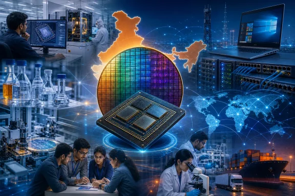
India’s Union Cabinet has approved Semicon 2.0, a ₹1,27,500 crore second phase of the India Semiconductor Mission intended to broaden the country’s chip ambitions from subsidising individual plants to building a domestic supply chain around them. The approval, announced July 15, extends the programme’s policy horizon from five years to 12.
Per the Prime Minister’s Office, the plan covers six areas: chip design; manufacturing equipment and inputs such as materials, chemicals and gases; new fabrication plants; advanced assembly, testing, marking and packaging; research; and workforce development. The government says the first silicon fab remains scheduled for commissioning in 2028.
Business Standard reports that the new scheme will offer up to 30 percent of project costs for semiconductor-equipment, specialty-chemical, gas and material makers that manufacture in India. Support for new fabs and packaging plants is being reduced versus Semicon 1.0, reflecting the government’s push to fund more of the upstream ecosystem rather than only final production facilities.
The reported framework includes 40 percent support for silicon fabs, 35 percent for other semiconductor fabs, 35 percent for advanced packaging, and 25 percent for conventional packaging. Operational guidelines are expected within two weeks.
For design companies, the plan reportedly proposes grants and equity support for smaller startups, while larger domestic companies could receive co-investment or royalty-based incentives. The policy emphasis is keeping chip intellectual property in India, not merely adding overseas-owned assembly capacity.
Micron, Kaynes and CG Semi have begun commercial production, while one additional project is expected to start during 2026. The country is therefore still at an early stage: packaging and testing are producing commercial output, while the flagship wafer-fabrication capacity remains years away.
The official announcement also says 105 startups and MSMEs have been given access to electronic design automation tools, while 24 chip-design projects have been approved for financial support. India’s government says 315 universities have trained roughly 68,000 students using industry-standard chip-design tooling.
Still, the move matters to the broader hardware market because supply-chain concentration remains a persistent risk for device makers and datacenter operators. If the programme produces viable fabs, advanced packaging capacity and local materials suppliers over the next decade, it could create another manufacturing and packaging option for global chip vendors.
For now, Semicon 2.0 is a long-term industrial-policy commitment rather than a near-term change to the Windows hardware market.
Per the Prime Minister’s Office, the plan covers six areas: chip design; manufacturing equipment and inputs such as materials, chemicals and gases; new fabrication plants; advanced assembly, testing, marking and packaging; research; and workforce development. The government says the first silicon fab remains scheduled for commissioning in 2028.
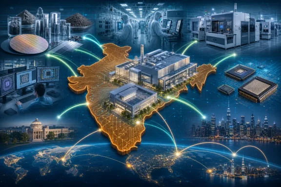 Incentives shift toward the supply chain
Business Standard reports that the new scheme will offer up to 30 percent of project costs for semiconductor-equipment, specialty-chemical, gas and material makers that manufacture in India. Support for new fabs and packaging plants is being reduced versus Semicon 1.0, reflecting the government’s push to fund more of the upstream ecosystem rather than only final production facilities.The reported framework includes 40 percent support for silicon fabs, 35 percent for other semiconductor fabs, 35 percent for advanced packaging, and 25 percent for conventional packaging. Operational guidelines are expected within two weeks.
For design companies, the plan reportedly proposes grants and equity support for smaller startups, while larger domestic companies could receive co-investment or royalty-based incentives. The policy emphasis is keeping chip intellectual property in India, not merely adding overseas-owned assembly capacity.
What India has so far
Semicon 1.0, approved in December 2021 with a ₹76,000 crore outlay, has approved 12 manufacturing projects worth more than ₹1.64 lakh crore in cumulative investment, according to the Prime Minister’s Office. Those include one silicon fab, a silicon-carbide fab, a gallium-nitride Micro LED display fab and nine packaging projects.Micron, Kaynes and CG Semi have begun commercial production, while one additional project is expected to start during 2026. The country is therefore still at an early stage: packaging and testing are producing commercial output, while the flagship wafer-fabrication capacity remains years away.
The official announcement also says 105 startups and MSMEs have been given access to electronic design automation tools, while 24 chip-design projects have been approved for financial support. India’s government says 315 universities have trained roughly 68,000 students using industry-standard chip-design tooling.
Why it matters for Windows users and IT buyers
The policy will not alter PC prices, Windows hardware availability, or enterprise procurement in the near term. India is not yet positioned to supply leading-edge CPUs, GPUs, DRAM or HBM used in mainstream PCs and AI servers. Its initial production is aimed more at automotive, industrial, telecom, power and consumer-electronics components, alongside packaging services.Still, the move matters to the broader hardware market because supply-chain concentration remains a persistent risk for device makers and datacenter operators. If the programme produces viable fabs, advanced packaging capacity and local materials suppliers over the next decade, it could create another manufacturing and packaging option for global chip vendors.
For now, Semicon 2.0 is a long-term industrial-policy commitment rather than a near-term change to the Windows hardware market.
References
- Primary source: the420.in
Published: 2026-07-15T13:25:05+00:00
Cabinet Clears ₹1.27 Lakh Crore for Semicon 2.0 Chip Mission - The420.in
Cabinet approves India Semiconductor Mission 2.0 with a ₹1.27 lakh crore outlay, targeting chip design, fabs, memory chips and talent development.the420.in - Related coverage: pmindia.gov.in
Cabinet approves Semicon 2.0 – Government delivers on its commitment for a long-term policy support to Semiconductors in India
Pm India Websitewww.pmindia.gov.in - Related coverage: ddindia.co.in
- Related coverage: business-standard.com
- Related coverage: m.economictimes.com
Cabinet approves India Semiconductor Mission 2.0; earmarks Rs 1.27 lakh crore for the project - The Economic Times
The Union Cabinet approved India Semiconductor Mission 2.0 with significant funding. A Rs 62,500 crore Mobile Phone Manufacturing Scheme was also cleared. These initiatives aim to boost domestic electronics manufacturing capabilities. The approvals are part of seven key decisions worth over...m.economictimes.com
- Related coverage: ndtvprofit.com