

Intel’s decision to pull Intel 14A forward by roughly a year is one of the clearest signals yet that its manufacturing turnaround is shifting from roadmap promises toward execution milestones. The company now expects risk production for internal products in the second half of 2027 and has committed to a high-volume manufacturing ramp in 2028, replacing an earlier schedule that placed risk production in 2028 and volume manufacturing in 2029.
For Windows PC users, enterprise buyers, and the broader semiconductor ecosystem, the timing matters far beyond a technical roadmap slide. Intel 14A is positioned as the company’s next major leading-edge manufacturing platform after Intel 18A, and its success could influence the performance, power efficiency, availability, and cost structure of future Intel processors and custom silicon built by Intel Foundry customers.
The update also arrives at a critical moment for Intel. The company is attempting to prove that it can execute on advanced nodes consistently, manufacture chips at meaningful volume, support outside customers as a genuine foundry, and compete in a market where process technology leadership is inseparable from AI, cloud, data center, and premium PC strategy.
Intel’s revised plan sets two distinct milestones for Intel 14A:
Risk production is the stage where a manufacturing technology begins producing limited silicon for validation, bring-up, yield learning, and early product development. It is not the same as broad commercial availability. Chips created during this phase are essential because they expose the real-world issues that simulations, test vehicles, and laboratory experiments can miss.
High-volume manufacturing, often shortened to HVM, is the more consequential milestone. It indicates that a node has reached the maturity needed to manufacture a large number of wafers economically and with yields sufficient to support shipping products. That is when a node can begin materially affecting the devices available to consumers, businesses, hyperscale cloud operators, and OEM partners.
Intel’s commitment to begin high-volume production in 2028 suggests that management believes the underlying technology, customer interest, and internal product plans justify making the expensive transition from development to sustained manufacturing capacity.
First, it compresses Intel’s product and manufacturing cadence. The company has already placed Intel 18A at the center of its near-term recovery, with the process intended to establish renewed credibility around leading-edge manufacturing. Intel 14A must now follow closely enough to sustain that momentum rather than leave a lengthy gap between major node introductions.
Second, it could make Intel more relevant to customers planning designs for the later part of the decade. Large semiconductor programs have long lead times. A company designing an advanced AI accelerator, networking ASIC, server processor, automotive compute device, or premium mobile SoC must choose a manufacturing partner years before retail hardware appears.
Third, the accelerated 14A schedule gives Intel Foundry a stronger pitch. It can present 14A not merely as an ambitious future technology, but as a process with a defined risk-production window, progressing design tools, an expanding intellectual-property portfolio, and a stated volume ramp plan.
The caveat is that a manufacturing schedule is still a forward-looking objective, not a guarantee. Advanced nodes are notoriously difficult to bring to high volume. Defect density, yield learning, equipment uptime, process variation, design-rule stability, packaging integration, and customer qualification can each alter a ramp.
A gate-all-around transistor surrounds the channel more completely, giving engineers stronger electrical control. That can help reduce leakage, enable lower operating voltages, and improve the balance between performance and power efficiency.
Intel 14A is expected to use RibbonFET 2, a second-generation implementation designed to extend the benefits introduced with Intel 18A. The goal is not just higher peak clock speeds. Modern chip design increasingly depends on improving performance within fixed power budgets, particularly in thin laptops, high-density servers, AI clusters, and fanless or thermally constrained devices.
For Windows PCs, that could eventually translate into processors that deliver better responsiveness and AI throughput without requiring a proportional increase in battery drain or cooling capacity. Of course, actual end-user gains will depend on architecture, memory, software, packaging, and OEM system design—not the manufacturing node alone.
Traditional chips route much of their power delivery through the same side of the silicon used for signal interconnects. As transistors become smaller and designs become denser, that routing becomes increasingly complex. Congestion can limit performance, complicate layout, and increase unwanted voltage variation.
Backside power delivery addresses the problem by moving power connections to the opposite side of the wafer. Intel 18A introduced PowerVia as its backside-power approach. Intel 14A’s PowerDirect is intended to go further with direct-contact power delivery techniques.
The potential benefits include:
High-NA EUV is strategically important because it can reduce the need for some of the complex multi-patterning steps otherwise required to create extremely dense structures. In theory, that can improve feature scaling and simplify portions of manufacturing. In practice, it also introduces new costs, process challenges, and operational demands.
Intel has spent years positioning itself as an early adopter of High-NA EUV. If Intel can use this equipment effectively in 14A production, it could gain a meaningful manufacturing advantage. Yet early adoption carries risk. New lithography systems must demonstrate not only technical capability, but also reliable throughput, predictable maintenance, stable resist performance, and acceptable cost per wafer.
That balance between technological ambition and manufacturing economics will be central to Intel 14A’s credibility.
However, semiconductor-node comparisons require care. Percentage claims depend on the conditions being measured:
This is why the strongest proof of Intel 14A will not be a process diagram or a presentation metric. It will be silicon: shipping processors, competitive yields, credible customer products, measurable performance, and systems that demonstrate clear advantages in the field.
A PDK provides the technical information, models, rules, and libraries that chip designers need to create a functional product for a specific manufacturing process. It helps electronic design automation tools understand the characteristics of the process and enables engineers to design circuits that can actually be manufactured.
A mature PDK typically includes elements such as:
A process node can have excellent transistor characteristics on paper yet still fail to attract customers if its design ecosystem is immature. Outside chip companies need reliable libraries, validated flows, qualified IP, responsive support, and confidence that the rules will not change late in development.
That is why Intel’s focus on PDK maturity and IP validation is arguably as important as its claims about density or transistor performance. Foundry customers buy a complete design-to-manufacturing experience, not a transistor alone.
Intel has stated that Intel 7, Intel 3, and Intel 18A exceeded internal volume targets, supported by improved factory usage, cycle times, and wafer availability. It has also indicated that 18A output is increasing to support products including Panther Lake and Wildcat Lake.
This matters because 18A serves as Intel’s operational rehearsal for the more ambitious 14A era.
Those disciplines include:
Still, 18A’s ramp remains the immediate test. A smooth 18A transition would support confidence in 14A. A difficult or delayed ramp would raise questions about whether the updated 14A timetable is too aggressive.
When a chipmaker uses its own process technology for its own products, it can coordinate decisions across the entire stack. Process engineers can work closely with CPU, GPU, AI accelerator, packaging, validation, and software teams. That does not eliminate risk, but it can reduce friction during the learning phase.
Internal product adoption can provide several advantages:
However, internal adoption alone will not fulfill Intel’s broader foundry ambitions. Outside customers must eventually view Intel as a trusted, neutral manufacturing partner with competitive technology, capacity, pricing, IP protection, packaging capability, and delivery reliability.
The company’s approach is a departure from an older model in which manufacturing technology was primarily optimized around Intel’s own processor roadmap. A third-party foundry must meet a broader range of needs. Customers may care about specialized I/O, radio-frequency integration, high-speed interfaces, dense SRAM, analog support, chiplet integration, automotive reliability, or advanced packaging.
Intel 14A therefore needs to be flexible enough for more than a single class of CPU design.
This distinction is central to Intel’s revised financial discipline. The company has made clear that leading-edge investment must be linked to real demand rather than open-ended capacity expansion. That is a rational change after years of heavy fab investment and uneven utilization.
The implications are straightforward:
Even so, the long-term implications for Windows hardware could be substantial.
Potential outcomes could include:
A mature 14A process could help Intel create processors that offer higher performance without expanding power consumption at the same rate. It may also support more sophisticated chiplet designs, allowing different parts of a processor package to be optimized for their own workloads.
Intel 14A could eventually support more capable combinations of CPU, GPU, and NPU resources. The best outcome would not simply be higher benchmark scores. It would be a Windows PC that can run more AI-assisted tasks locally, respond faster, protect sensitive data by reducing cloud dependence, and do so without compromising battery life.
That philosophy is important because leading-edge fabrication is extraordinarily expensive. New fabs, lithography tools, advanced packaging lines, materials infrastructure, talent, and research all require enormous up-front spending. A foundry cannot thrive simply by possessing impressive technology; it needs enough customer demand to keep factories productive and financially sustainable.
Intel’s updated 14A schedule indicates that management sees a stronger basis for moving ahead. The advancement of risk production to 2027 and volume ramp to 2028 suggests confidence in the node’s development progress and in the relevance of the technology to future products.
But the true test will be whether that confidence is supported by tangible outcomes: stable PDK releases, qualified IP, successful internal tape-outs, credible customer commitments, improving yields, and eventually shipping chips.
The technology itself is ambitious. RibbonFET 2, PowerDirect, and High-NA EUV position Intel 14A as more than a routine shrink, with the potential to improve performance, efficiency, density, and design flexibility. The PDK and IP work underway will be equally important, because modern foundry competition is decided by the quality of the complete ecosystem as much as by transistor innovation.
For the Windows ecosystem, the immediate impact will be limited. The long-term impact could be substantial. If Intel executes, 14A may help underpin a new generation of more efficient AI PCs, stronger desktop processors, advanced server silicon, and custom chips from external customers.
For now, Intel 14A is best understood as a high-stakes commitment rather than a finished victory. The accelerated schedule is promising, but the road from risk production to sustained high-volume manufacturing remains where Intel must prove that its renewed manufacturing strategy can deliver.
For Windows PC users, enterprise buyers, and the broader semiconductor ecosystem, the timing matters far beyond a technical roadmap slide. Intel 14A is positioned as the company’s next major leading-edge manufacturing platform after Intel 18A, and its success could influence the performance, power efficiency, availability, and cost structure of future Intel processors and custom silicon built by Intel Foundry customers.
The update also arrives at a critical moment for Intel. The company is attempting to prove that it can execute on advanced nodes consistently, manufacture chips at meaningful volume, support outside customers as a genuine foundry, and compete in a market where process technology leadership is inseparable from AI, cloud, data center, and premium PC strategy.
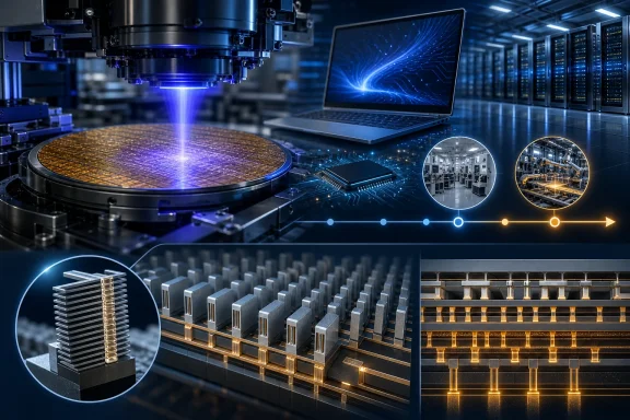 Intel 14A Moves From a Long-Term Promise to a Nearer Manufacturing Target
Intel’s revised plan sets two distinct milestones for Intel 14A:- Risk production for internal products in the second half of 2027
- High-volume production in 2028
Risk production is the stage where a manufacturing technology begins producing limited silicon for validation, bring-up, yield learning, and early product development. It is not the same as broad commercial availability. Chips created during this phase are essential because they expose the real-world issues that simulations, test vehicles, and laboratory experiments can miss.
High-volume manufacturing, often shortened to HVM, is the more consequential milestone. It indicates that a node has reached the maturity needed to manufacture a large number of wafers economically and with yields sufficient to support shipping products. That is when a node can begin materially affecting the devices available to consumers, businesses, hyperscale cloud operators, and OEM partners.
Intel’s commitment to begin high-volume production in 2028 suggests that management believes the underlying technology, customer interest, and internal product plans justify making the expensive transition from development to sustained manufacturing capacity.
Why the New Timeline Is Important
A move from a 2029 volume target to 2028 is significant for several reasons.First, it compresses Intel’s product and manufacturing cadence. The company has already placed Intel 18A at the center of its near-term recovery, with the process intended to establish renewed credibility around leading-edge manufacturing. Intel 14A must now follow closely enough to sustain that momentum rather than leave a lengthy gap between major node introductions.
Second, it could make Intel more relevant to customers planning designs for the later part of the decade. Large semiconductor programs have long lead times. A company designing an advanced AI accelerator, networking ASIC, server processor, automotive compute device, or premium mobile SoC must choose a manufacturing partner years before retail hardware appears.
Third, the accelerated 14A schedule gives Intel Foundry a stronger pitch. It can present 14A not merely as an ambitious future technology, but as a process with a defined risk-production window, progressing design tools, an expanding intellectual-property portfolio, and a stated volume ramp plan.
The caveat is that a manufacturing schedule is still a forward-looking objective, not a guarantee. Advanced nodes are notoriously difficult to bring to high volume. Defect density, yield learning, equipment uptime, process variation, design-rule stability, packaging integration, and customer qualification can each alter a ramp.
The Technology Behind Intel 14A
Intel 14A is not simply a smaller version of Intel 18A. It is intended to be a more advanced process platform with major changes to transistor architecture, power delivery, lithography, and design flexibility.RibbonFET 2 and the Next Stage of Gate-All-Around Transistors
At the transistor level, Intel 14A is expected to build on RibbonFET, Intel’s gate-all-around transistor architecture. Gate-all-around designs replace the traditional FinFET approach used for many previous generations of high-performance processors.A gate-all-around transistor surrounds the channel more completely, giving engineers stronger electrical control. That can help reduce leakage, enable lower operating voltages, and improve the balance between performance and power efficiency.
Intel 14A is expected to use RibbonFET 2, a second-generation implementation designed to extend the benefits introduced with Intel 18A. The goal is not just higher peak clock speeds. Modern chip design increasingly depends on improving performance within fixed power budgets, particularly in thin laptops, high-density servers, AI clusters, and fanless or thermally constrained devices.
For Windows PCs, that could eventually translate into processors that deliver better responsiveness and AI throughput without requiring a proportional increase in battery drain or cooling capacity. Of course, actual end-user gains will depend on architecture, memory, software, packaging, and OEM system design—not the manufacturing node alone.
PowerDirect and Backside Power Delivery
Intel 14A is also expected to advance backside power delivery through PowerDirect. This continues the broader industry move toward separating power-routing and signal-routing functions more effectively within a chip.Traditional chips route much of their power delivery through the same side of the silicon used for signal interconnects. As transistors become smaller and designs become denser, that routing becomes increasingly complex. Congestion can limit performance, complicate layout, and increase unwanted voltage variation.
Backside power delivery addresses the problem by moving power connections to the opposite side of the wafer. Intel 18A introduced PowerVia as its backside-power approach. Intel 14A’s PowerDirect is intended to go further with direct-contact power delivery techniques.
The potential benefits include:
- More room for signal wiring on the front side of the chip
- Lower resistance in the power-delivery network
- Reduced voltage droop under demanding workloads
- Better transistor utilization within dense logic blocks
- Greater flexibility for designers targeting high-frequency compute sections
High-NA EUV Lithography Enters the Picture
Intel 14A is also associated with high-numerical-aperture extreme ultraviolet lithography, commonly called High-NA EUV. This equipment is designed to pattern smaller and more precise features than conventional EUV systems.High-NA EUV is strategically important because it can reduce the need for some of the complex multi-patterning steps otherwise required to create extremely dense structures. In theory, that can improve feature scaling and simplify portions of manufacturing. In practice, it also introduces new costs, process challenges, and operational demands.
Intel has spent years positioning itself as an early adopter of High-NA EUV. If Intel can use this equipment effectively in 14A production, it could gain a meaningful manufacturing advantage. Yet early adoption carries risk. New lithography systems must demonstrate not only technical capability, but also reliable throughput, predictable maintenance, stable resist performance, and acceptable cost per wafer.
That balance between technological ambition and manufacturing economics will be central to Intel 14A’s credibility.
Intel’s Claimed 14A Improvements Need Careful Context
Intel has positioned 14A as a substantial advance over Intel 18A, with internal projections indicating gains in performance per watt, lower power at equivalent performance, and higher density. These targets are promising, particularly for markets where energy efficiency has become as important as raw performance.However, semiconductor-node comparisons require care. Percentage claims depend on the conditions being measured:
- Is performance measured at the same power?
- Is power measured at the same performance?
- Which standard-cell libraries are used?
- Are density comparisons based on logic density, SRAM density, or a particular design style?
- Does the comparison account for chip architecture and packaging?
- Are results from test circuits representative of shipping products?
This is why the strongest proof of Intel 14A will not be a process diagram or a presentation metric. It will be silicon: shipping processors, competitive yields, credible customer products, measurable performance, and systems that demonstrate clear advantages in the field.
PDK Progress Is a Crucial Foundry Signal
Intel has already released PDK 0.5 for 14A and expects PDK 0.9 to arrive in October. PDK stands for process design kit, and it is one of the most important but least visible elements of foundry success.A PDK provides the technical information, models, rules, and libraries that chip designers need to create a functional product for a specific manufacturing process. It helps electronic design automation tools understand the characteristics of the process and enables engineers to design circuits that can actually be manufactured.
A mature PDK typically includes elements such as:
- Design rules and physical-layout constraints
- Transistor models for timing and power analysis
- Reliability guidance
- Process corners and variation models
- Standard-cell libraries
- SRAM compiler support
- I/O and interface options
- Verification collateral
- Compatibility data for design tools
A process node can have excellent transistor characteristics on paper yet still fail to attract customers if its design ecosystem is immature. Outside chip companies need reliable libraries, validated flows, qualified IP, responsive support, and confidence that the rules will not change late in development.
That is why Intel’s focus on PDK maturity and IP validation is arguably as important as its claims about density or transistor performance. Foundry customers buy a complete design-to-manufacturing experience, not a transistor alone.
Intel 18A Is the Necessary Proving Ground
Intel 14A cannot be evaluated in isolation. Its credibility depends heavily on the progress of Intel 18A, the preceding node that introduced RibbonFET and PowerVia into Intel’s leading-edge manufacturing strategy.Intel has stated that Intel 7, Intel 3, and Intel 18A exceeded internal volume targets, supported by improved factory usage, cycle times, and wafer availability. It has also indicated that 18A output is increasing to support products including Panther Lake and Wildcat Lake.
This matters because 18A serves as Intel’s operational rehearsal for the more ambitious 14A era.
Lessons Intel Must Carry Forward
The key question is not only whether 18A can reach volume. It is whether Intel can institutionalize the disciplines needed to repeat the achievement with 14A.Those disciplines include:
- Maintaining stable design rules early enough for product teams
- Improving yield at a predictable pace
- Preventing late-stage process changes
- Managing equipment capacity and factory cycle times
- Coordinating product, foundry, packaging, and design teams
- Supporting external customers without prioritizing Intel products unfairly
- Turning technical progress into sustainable manufacturing margins
Still, 18A’s ramp remains the immediate test. A smooth 18A transition would support confidence in 14A. A difficult or delayed ramp would raise questions about whether the updated 14A timetable is too aggressive.
Internal Products Could De-Risk Intel 14A
Intel’s decision to begin 14A risk production with internal products is strategically sensible. Internal designs give the company more control over the initial ramp, product schedule, design methodology, and engineering feedback loop.When a chipmaker uses its own process technology for its own products, it can coordinate decisions across the entire stack. Process engineers can work closely with CPU, GPU, AI accelerator, packaging, validation, and software teams. That does not eliminate risk, but it can reduce friction during the learning phase.
Internal product adoption can provide several advantages:
- Early and predictable wafer demand
- Faster feedback on design and manufacturing issues
- Better alignment between process capabilities and chip architecture
- A public proof point for external customers
- A stronger business case for manufacturing investment
However, internal adoption alone will not fulfill Intel’s broader foundry ambitions. Outside customers must eventually view Intel as a trusted, neutral manufacturing partner with competitive technology, capacity, pricing, IP protection, packaging capability, and delivery reliability.
External Customer Momentum Is Encouraging but Still Unproven
Intel management has described increasing customer engagement for 14A and said the technology is being developed with a wider range of customers in mind. That is encouraging, especially because Intel’s newer foundry strategy emphasizes customer collaboration earlier in the process-development cycle.The company’s approach is a departure from an older model in which manufacturing technology was primarily optimized around Intel’s own processor roadmap. A third-party foundry must meet a broader range of needs. Customers may care about specialized I/O, radio-frequency integration, high-speed interfaces, dense SRAM, analog support, chiplet integration, automotive reliability, or advanced packaging.
Intel 14A therefore needs to be flexible enough for more than a single class of CPU design.
The Unnamed Customer Challenge
The important limitation is that major 14A customer commitments remain largely undisclosed. Interest, test chips, PDK evaluations, and engineering engagements are meaningful, but they are not the same as a signed production contract with substantial wafer volume.This distinction is central to Intel’s revised financial discipline. The company has made clear that leading-edge investment must be linked to real demand rather than open-ended capacity expansion. That is a rational change after years of heavy fab investment and uneven utilization.
The implications are straightforward:
- A major external win would validate Intel 14A as a true foundry platform.
- Multiple smaller engagements would demonstrate ecosystem progress but may not justify the same scale of capital investment.
- Failure to secure enough committed volume could constrain the pace of expansion even if the technology itself performs well.
What It Could Mean for Future Windows PCs
Intel 14A is not expected to affect mainstream Windows laptops or desktops immediately. The first risk-production period begins in the second half of 2027, while high-volume manufacturing is planned for 2028. Products built on the node would likely arrive after the manufacturing ramp is well underway.Even so, the long-term implications for Windows hardware could be substantial.
Better Efficiency for Mobile Systems
Modern Windows notebooks increasingly need to balance CPU performance, integrated graphics, neural processing, media engines, memory bandwidth, and battery life. A more efficient node gives Intel product teams more flexibility to optimize all of those elements.Potential outcomes could include:
- Lower power consumption during everyday productivity work
- Better sustained performance in thin-and-light laptops
- More headroom for local AI workloads
- Improved integrated graphics behavior within mobile power limits
- Reduced cooling requirements for premium ultrabooks
More Competitive Desktop and Gaming Designs
Desktop processors have different priorities. Performance, cache capacity, peak clocks, I/O, graphics integration, and platform cost often matter more than battery life. But power efficiency remains valuable, particularly as high-end PCs face increasingly large cooling and power-delivery requirements.A mature 14A process could help Intel create processors that offer higher performance without expanding power consumption at the same rate. It may also support more sophisticated chiplet designs, allowing different parts of a processor package to be optimized for their own workloads.
Stronger AI PC and Edge Computing Options
The AI PC market is still evolving, but the manufacturing requirements are becoming clearer. Local AI features demand more compute performance in compact systems, often under tight thermal limits. That makes node efficiency increasingly important.Intel 14A could eventually support more capable combinations of CPU, GPU, and NPU resources. The best outcome would not simply be higher benchmark scores. It would be a Windows PC that can run more AI-assisted tasks locally, respond faster, protect sensitive data by reducing cloud dependence, and do so without compromising battery life.
The Risks Intel Must Manage
Intel 14A’s revised schedule is ambitious, and ambition alone does not guarantee execution. Several risks deserve close attention.Manufacturing Complexity
High-NA EUV, second-generation gate-all-around transistors, advanced backside power delivery, and next-generation design enablement make 14A technically ambitious. Each can introduce new manufacturing challenges. Combining them increases the need for disciplined process integration.Yield and Cost Pressure
A node can technically work without being economically viable at scale. If yields take too long to improve, Intel may face higher costs per good die, weaker gross margins, limited supply, or a slower rollout for internal and external customers.Customer-Commitment Risk
Intel Foundry needs external design wins, especially at the leading edge. If customers do not commit meaningful volume, Intel may struggle to justify the full scale of investment required for 14A capacity.Competitive Response
The foundry market will not stand still until 2028. Rival manufacturers will continue advancing their own process technologies, packaging capabilities, and customer ecosystems. Intel must be competitive not only in density and performance, but also in schedule, cost, service, IP support, and geographic supply-chain strategy.Product Execution
A strong manufacturing node does not automatically create a strong processor. Intel’s product teams must pair 14A with compelling architectures, clear platform roadmaps, attractive pricing, and reliable OEM availability. The company needs technical leadership at both the process and product levels.A More Disciplined Intel Foundry Strategy
The most notable aspect of the 14A update may be the shift in Intel’s tone. The company is no longer presenting manufacturing expansion as an automatic outcome of technology development. Instead, it is emphasizing disciplined execution, customer demand, internal product needs, and economically justified investment.That philosophy is important because leading-edge fabrication is extraordinarily expensive. New fabs, lithography tools, advanced packaging lines, materials infrastructure, talent, and research all require enormous up-front spending. A foundry cannot thrive simply by possessing impressive technology; it needs enough customer demand to keep factories productive and financially sustainable.
Intel’s updated 14A schedule indicates that management sees a stronger basis for moving ahead. The advancement of risk production to 2027 and volume ramp to 2028 suggests confidence in the node’s development progress and in the relevance of the technology to future products.
But the true test will be whether that confidence is supported by tangible outcomes: stable PDK releases, qualified IP, successful internal tape-outs, credible customer commitments, improving yields, and eventually shipping chips.
The Bottom Line
Intel 14A entering high-volume production in 2028 would mark a major milestone in the company’s attempt to reclaim manufacturing leadership and establish Intel Foundry as a credible alternative for leading-edge chip production. Pulling risk production into the second half of 2027 is an especially meaningful change because it gives internal product teams and prospective customers an earlier path to validate real silicon.The technology itself is ambitious. RibbonFET 2, PowerDirect, and High-NA EUV position Intel 14A as more than a routine shrink, with the potential to improve performance, efficiency, density, and design flexibility. The PDK and IP work underway will be equally important, because modern foundry competition is decided by the quality of the complete ecosystem as much as by transistor innovation.
For the Windows ecosystem, the immediate impact will be limited. The long-term impact could be substantial. If Intel executes, 14A may help underpin a new generation of more efficient AI PCs, stronger desktop processors, advanced server silicon, and custom chips from external customers.
For now, Intel 14A is best understood as a high-stakes commitment rather than a finished victory. The accelerated schedule is promising, but the road from risk production to sustained high-volume manufacturing remains where Intel must prove that its renewed manufacturing strategy can deliver.
References
- Primary source: Wccftech
Published: 2026-07-23T21:38:54+00:00
Loading…
wccftech.com - Related coverage: techspot.com
Intel says 14A is on track for 2028 risk production, 10A and 7A now in development | TechSpot
Speaking at J.P. Morgan' 54th annual Global Technology, Media and Communications Conference in Boston, Tan revealed that development of Intel's 14A process node is progressing as planned,...www.techspot.com - Related coverage: trendforce.com
[News] Intel Pulls Forward 14A Timeline by One Year, Targeting 2028 Mass Production Near TSMC’s Roadmap
As Intel delivered stronger-than-expected second-quarter results, reportedly posting its fastest quarterly revenue growth since 2011 and hiked its 202...www.trendforce.com