
The distinction is more than semantic. Architect Labs’ August 27 announcement says its scaled-down Redwood Nano design runs Qwen3-0.6B on an AMD Versal VPK180 FPGA at 250 MHz, achieving 12.1 tokens per second end to end. The company then projects how an ASIC implementation on Samsung’s 8 nm process would compare with a measured Jetson Orin Nano baseline. Business Insider’s reporting, republished by CNCB News, and a separate examination from R&D World both identify manufacturing as the uncompleted step.
That makes the submitted Citybiz account materially misleading on the benchmark. It describes Redwood as delivering “75x greater throughput” and “4x higher performance-per-watt.” Architect Labs’ own technical post instead claims 1.75 times decode throughput, 1.9 times lower power use, and a 3.4-fold performance-per-watt gain against the measured Jetson baseline on the same model. The 75x figure is not supported by Architect Labs’ published announcement or the independent follow-up coverage reviewed so far.
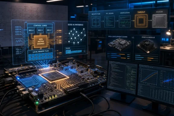 Redwood’s two-week claim covers more than RTL generation
“AI-designed chip” is becoming a loose term. In many cases it means using generative tools to assist a hardware engineer with isolated RTL modules, testbenches, or placement-and-routing work. Architect Labs’ claim is broader: two human architects supplied a high-level specification, then its in-house platform generated the performance model, RTL, UVM verification environments, SystemVerilog assertions, formal proofs, firmware, host drivers, and compute kernels.
That breadth is what makes Redwood worth watching. A hardware program can be delayed even when the core datapath is sound, because verification, low-level software, and performance tuning are separate queues with different owners. Architect says it instead uses the specification as a common source of truth and regenerates downstream artifacts as it explores architectural changes. It reports 48-hour cycles from a revised design direction to a re-verified FPGA deployment.
For teams building robots, industrial vision systems, drones, and other edge hardware, the potential benefit is straightforward: a model architecture, quantization approach, memory arrangement, and accelerator kernel could be optimized together instead of forcing software onto a chip planned years earlier. The approach is particularly suited to single-batch, latency-sensitive inference rather than the high-throughput batch processing that dominates data-center GPU benchmarks.
Architect Labs says Redwood uses a tile-based spatial-dataflow architecture. Each tile combines a RISC-V control core, an INT8 matrix engine, a vector engine, and 512 KB of local memory. The design keeps work close to memory, uses DMA engines for external transfers, and pushes scheduling decisions into software. It also implements FlashAttention-4-related softmax behavior through existing vector resources rather than dedicated hardware, an engineering trade-off aimed at saving chip area.
Those choices are credible design ideas, but they do not independently validate the company’s automation claims. The published evidence remains Architect Labs’ own repository history, coverage figures, and FPGA test results. No outside lab has yet published a reproduction of the full generation flow, an audit of the claimed zero-human-intervention work below the specification, or a comparison using fabricated Redwood hardware.
FPGA success does not settle an ASIC’s power, timing, or yield
An FPGA is a vital proving ground: it runs real software and exposes integration mistakes that simulation can miss. It is also programmable hardware with a very different area, clocking, memory, power, and physical-design profile from a purpose-built ASIC. Converting an RTL design that runs on an AMD Versal FPGA into a chip layout ready for a foundry remains substantial engineering work.
Architect Labs acknowledges that boundary explicitly. Its published roadmap calls for taking Redwood through full GDSII layout and a tapeout at TSMC, followed by post-silicon validation. Business Insider reported that CEO Ebrahim Hussain said the company had not fixed a manufacturing date because its AI system was still refining the design.
The company’s 95%-plus code and functional coverage claim also deserves careful reading. Coverage is an important measure of what a verification environment has exercised; it is not proof that every bug is absent. Architect says every block through the SoC level met that threshold, combining commercial EDA tools, its proprietary formal engine, and hardware-in-the-loop testing, while the first RTL transfer from simulation to the FPGA had zero bugs. That is a promising initial result, not a substitute for silicon bring-up, characterization across voltage and temperature ranges, reliability testing, or production yield data.
UC Santa Cruz computer science and engineering professor Matthew Guthaus made the key point in Business Insider’s reporting: AI can be effective in many parts of chip design, but it can also make mistakes that need close supervision and checking. In chip development, errors that surface after tapeout can cost millions of dollars and months of schedule. Automating the checks is useful only if the checks cover the failures that matter.
The Jetson comparison is narrower than the marketing suggests
Architect Labs selected Nvidia’s Jetson Orin Nano because it is an established platform for compact edge AI systems. That is a reasonable target for a low-power accelerator, but it is not a direct replacement test for the complete Jetson product.
Jetson Orin Nano is a system-on-module backed by Nvidia’s CUDA, TensorRT, JetPack, drivers, developer tools, media support, and broad peripheral integration. Redwood Nano, by contrast, is presently a custom inference design instantiated in an AMD FPGA, executing one named test workload: Qwen3-0.6B. The company says external memory traffic is modularized around standard AXI4 interfaces and that the design could become a chiplet or integrate into a wider system-on-chip, but it has not announced a module, board, SDK, operating-system support matrix, price, availability date, or production customer deployment.
The measurement methodology also matters. Architect says it compared a measured Jetson baseline with an ASIC projection calibrated from its FPGA results at a comparable 8 nm process class. R&D World describes the resulting comparison as 1.75 times projected throughput at roughly 47% less power, yielding the claimed 3.4 times performance-per-watt. This does not show 75 times more throughput, and it does not show how Redwood would perform across vision models, multimodal workloads, different batch sizes, long-context inference, thermally constrained enclosures, or Nvidia-optimized software.
For enterprises, the right conclusion is not to delay an edge deployment in anticipation of a Redwood part. Jetson, AMD, Qualcomm, Ambarella, Hailo, and other established vendors provide hardware that can be purchased, characterized, supported, and integrated today. Architect Labs has demonstrated a design process and an FPGA runtime, not yet a product with those properties.
Hardware-software co-design is the practical breakthrough to watch
The real test of Architect Labs’ work is whether its flow can make custom silicon less risky before the foundry phase, not whether it can issue a dramatic benchmark claim. Traditional hardware programs often freeze major choices early because downstream changes are expensive. If a co-design platform can cheaply regenerate RTL, test infrastructure, firmware, and kernels when the target model changes, it can shift what workloads are economical to customize.
Architect Labs says its AI agents use shared FPGA access to reduce some optimization runs from roughly 15 hours to 15–30 minutes. It also says a Qwen3 model running as an API endpoint on Redwood found timing and kernel improvements for the next generation of the accelerator. That “recursive self-improvement” language runs ahead of the public evidence, but the smaller underlying claim is plausible: an LLM can propose optimizations for software and hardware artifacts when a broader system measures and verifies them.
The company’s most concrete proof point will be a taped-out Redwood chip that meets its projected power, performance, and area targets in independent measurements. Until then, the two-week milestone should be read as a credible FPGA-based demonstration of automated hardware-software co-design—and a warning that Citybiz’s 75x performance claim is not borne out by the primary record.