India’s Union Cabinet has approved
₹1.275 trillion for Semiconductor Mission 2.0, widening the country’s chip strategy beyond fabrication plants to cover domestic processor design, manufacturing equipment, specialty materials, advanced packaging, research and workforce training. The decision matters well beyond India: PCs, servers, networking hardware and Windows devices all depend on a semiconductor supply chain still concentrated in a handful of countries and companies.
The Cabinet approved the program on July 15, according to the Press Information Bureau and reporting from
Mint. Electronics and Information Technology Minister Ashwini Vaishnaw said detailed operational guidelines are expected within two weeks, making those rules the next key milestone for companies considering applications.
Semicon 2.0 follows the ₹760 billion India Semiconductor Mission launched in December 2021. That first phase produced approvals for 12 manufacturing projects representing more than ₹1.6 trillion in planned investment, but the new program is designed to address the ecosystem surrounding those factories rather than simply subsidize more production capacity.
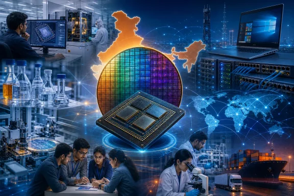 India Moves Beyond the Fab Announcement
Large fabrication plants attract attention because of their cost and strategic value, but they cannot operate in isolation. Chip production requires specialized gases, chemicals, substrates, precision machinery, intellectual property, trained engineers and facilities capable of testing and packaging finished silicon.
Semicon 2.0 organizes that problem around six areas: chip design, equipment and materials, fabrication, packaging, research and development, and talent. The scope signals that New Delhi wants to build more of the semiconductor value chain domestically instead of importing the inputs needed to run Indian fabs.
Chip design receives a particularly prominent role. The government says 105 startups began developing chips under the earlier mission, while the new phase will support semiconductor intellectual property, complete chip designs and the systems built around them.
Smaller design companies could receive a combination of grants and government equity investment, according to
Business Standard. Medium-sized and larger Indian companies may instead be offered co-investment or royalty-based arrangements, with the policy structured to keep strategically important intellectual property in India.
That represents a more ambitious goal than contract manufacturing. A country hosting factories may still depend on overseas companies for the architecture, electronic design automation tools and reusable IP blocks that determine what those factories produce. Semicon 2.0 is explicitly attempting to narrow at least part of that gap.
Incentives Shift Toward the Missing Pieces
The new funding structure reduces support for some established categories while creating incentives for equipment, chemicals, gases and semiconductor materials. Eligible suppliers in those areas could receive up to 30% of project costs.
For fabrication projects, support is expected to fall from the flat 50% available under the first mission. Silicon fabs could receive incentives covering up to 40% of project costs, while compound semiconductor and other fabrication projects could qualify for up to 35%.
Packaging incentives are also becoming more selective. Advanced packaging projects could receive support of up to 35%, while conventional Assembly, Testing, Marking and Packaging or Outsourced Semiconductor Assembly and Test facilities would be eligible for up to 25%.
The reductions do not necessarily indicate that fabrication and packaging have become less important. Rather, the government is spreading the ₹1.275 trillion allocation across more links in the chain now that India has an initial group of approved manufacturing projects.
Research and skills receive potentially deeper combined support. Central and state incentives could cover as much as 75% of eligible costs for advanced semiconductor R&D, while a similar structure is planned for universities, startups and other organizations training design and manufacturing specialists.
India says 315 universities are already using industry-standard Electronic Design Automation tools to teach chip design, reaching about 68,000 students. Semicon 2.0 is intended to expand that pipeline into specialized areas including clean-room operations, fab construction and semiconductor manufacturing.
Advanced Packaging Becomes a Strategic Target
For the PC industry, the focus on advanced packaging may prove just as consequential as the effort to attract fabs. Modern processors increasingly combine multiple pieces of silicon rather than relying on one monolithic die, making packaging technology central to performance, power efficiency and production yield.
AMD’s Ryzen processors have helped popularize
chiplet designs in Windows PCs, while Intel has adopted technologies such as Foveros for products that combine compute, graphics and input-output components. AI accelerators and high-performance server processors also rely on increasingly complex links between processing dies and high-bandwidth memory.
India already has momentum in assembly and testing, including Micron’s facility at Sanand, Gujarat. Semicon 2.0’s distinction between conventional and advanced packaging shows that policy is now being directed toward higher-value manufacturing rather than maximizing the number of basic assembly operations.
The first phase approved nine packaging facilities, alongside one silicon fab and projects involving compound semiconductors and display technology. Three of the 12 approved semiconductor plants have reportedly entered commercial production, although India’s first major silicon wafer fab is not expected to be commissioned until 2028.
That timetable is an important constraint. Cabinet approval establishes the financial framework, but semiconductor factories take years to construct, equip, qualify and bring to stable production. The success of Semicon 2.0 will be measured less by announced investment totals than by production yields, customer orders and the number of locally sourced inputs that factories can actually use.
Windows Hardware Gains Another Supply-Chain Option
Semicon 2.0 will not immediately produce a new class of Indian-designed Windows processors, nor is it likely to displace TSMC, Samsung or Intel Foundry at leading-edge nodes in the near term. India’s initial manufacturing opportunity is broader and more practical: automotive controllers, power-management chips, communications components, display electronics, sensors, industrial devices and mature-node silicon used throughout PCs and servers.
A Windows laptop contains far more chips than its AMD, Intel or Qualcomm processor. Storage controllers, wireless modules, USB controllers, embedded controllers, power-management components and display interfaces can all become production bottlenecks, as PC manufacturers discovered during the pandemic-era semiconductor shortage.
Additional geographically distributed capacity could therefore improve resilience even when it does not manufacture the primary CPU. Indian packaging, materials and component plants could also give hardware vendors another sourcing option as governments and manufacturers try to reduce exposure to single-region disruptions.
The parallel approval of a ₹625 billion Mobile Phone Manufacturing Scheme reinforces that objective. Although aimed at smartphones, the scheme rewards domestic sourcing, product design and locally developed intellectual property—capabilities that overlap with the supply chains serving tablets, Arm-based Windows systems, connectivity modules and consumer electronics.
Government projections attach large numbers to the semiconductor program: ₹4 trillion in investment, ₹2 trillion in production and ₹1 trillion in exports. Those remain targets rather than delivered outcomes, and the program’s detailed application criteria will determine whether funding attracts durable technology transfer or primarily subsidizes facilities dependent on imported machinery and know-how.
Semicon 2.0 nevertheless marks a clear change in emphasis. India is no longer treating the fab as the whole semiconductor strategy; it is funding the
designs, tools, materials, packaging and people required to keep one running. For Windows device makers and enterprise hardware buyers, the practical result will emerge gradually—first through components and packaging, and only later through any processors bearing genuinely Indian intellectual property.

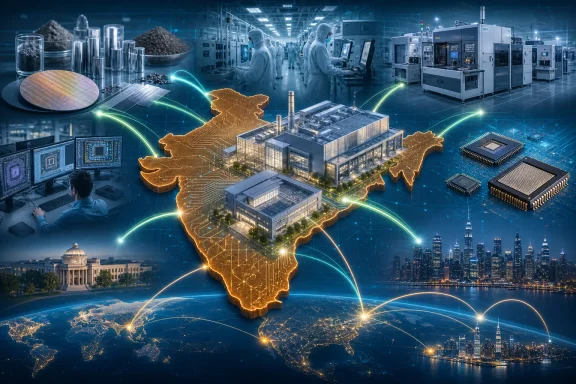 Incentives shift toward the supply chain
