
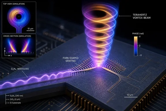
 The breakthrough: a terahertz vortex laser that lives on one chip
The notable achievement is not simply producing terahertz radiation. It is bringing together several normally separate functions—generation, in-plane guidance, and free-space wavefront shaping—in one semiconductor structure. That integration matters because practical terahertz hardware has historically been dominated by system-level compromises: sources, optics, mounts, and measurement paths can all be individually impressive while the combined instrument remains large and finicky.
Yan’s group attacks that problem at the point where a guided terahertz field leaves the chip. Rather than directing the wave toward a separately aligned spiral phase plate, spatial light modulator, metasurface, or other external shaping element, the device incorporates a fork-shaped grating directly into the semiconductor platform. The grating diffracts a portion of the guided signal upward as a vortex beam while leaving the rest of the guided wave comparatively undisturbed. The AIP description says the researchers then characterized the output spectrum, optical power, polarization, and vortex properties.
That is an important distinction. A lab demonstration that makes a twisted beam with a chain of external components proves a physical effect. A monolithically integrated terahertz vortex laser begins to address the engineering challenge of packaging that effect into something that can be reproduced, miniaturized, and eventually combined with control and readout electronics.
Gangyi Xu, one of the study’s authors, framed the advance as a move away from carefully aligned multi-component optical benches and toward “putting an entire terahertz optical system onto a semiconductor chip.” That ambition should not be confused with a finished commercial subsystem, but it is exactly the kind of systems-level direction that terahertz photonics needs. AIP’s account also reports the team’s goal of later adding modulation and detection functions, as well as switching dynamically among vortex and other structured-light states.
Background: why terahertz photonics has been hard to shrink
Terahertz radiation occupies the electromagnetic territory between conventional microwaves and infrared light. It has attracted sustained attention because it can support sensing, imaging, spectroscopy, communications, and materials research, but it also comes with stubborn device and propagation challenges.
At these frequencies, systems can interact with molecular signatures in ways that are valuable for spectroscopic analysis, while their shorter wavelengths relative to microwave systems can support finer spatial detail. The U.S. National Institute of Standards and Technology notes that terahertz imaging and spectroscopy have demonstrated potential in areas including non-ionizing screening for concealed contraband, industrial processing, and remote chemical identification. NIST’s terahertz imaging overview emphasizes both the application opportunities and the continuing importance of detector, optical, calibration, and test-bed development.
For communications, the appeal is equally understandable. The terahertz spectrum contains large swaths of underused bandwidth, and the short wavelength can support highly directional beams and high spatial resolution. A comprehensive review of terahertz communications and sensing describes the band as a potential enabler for future systems because of its available spectrum and resolution advantages, while also stressing major challenges such as atmospheric absorption, free-space loss, weather effects, beam alignment, and hardware limitations. The review makes clear that high-frequency capacity does not erase the need for robust transceiver design and careful propagation engineering.
This is why the phrase “terahertz gap” remains useful. The issue is not that terahertz waves are scientifically mysterious. It is that generating, detecting, manipulating, packaging, and measuring them efficiently has been much less straightforward than doing the equivalent jobs at radio, microwave, or optical frequencies.
The bulk-optics bottleneck
Traditional terahertz beam-shaping experiments often rely on external components. These might include lenses, phase plates, gratings, mirrors, polarization optics, antennas, and mechanical stages. Each part can add insertion loss, occupy space, introduce alignment sensitivity, and complicate calibration.
For structured beams in particular, the challenge grows quickly. A vortex beam is defined by a spatially varying phase structure, so the shaping hardware must preserve a precise relationship across the wavefront. A slight displacement, angular mismatch, or environmental disturbance can degrade mode purity or alter the output pattern.
The broader vortex-beam literature has long documented a transition from bulky diffractive and holographic components toward thinner, planar, and integrated approaches. An Optica review of vortex-beam generation and detection describes vortex beams as structured beams carrying orbital angular momentum and explicitly traces generation technologies from bulk diffractive elements to planar alternatives.
Yan and colleagues’ work is therefore timely because it pursues integration at the terahertz source itself rather than treating wavefront control as an external accessory.
What makes a vortex beam different
A vortex beam is a structured electromagnetic beam whose phase winds around its central axis. Instead of every point across a wavefront having the same phase relationship, the phase changes azimuthally as one travels around the beam center.
The result is often described visually as a corkscrew-like or helical wavefront. At the center lies a phase singularity, where the phase is not defined in the usual sense and the idealized intensity profile typically exhibits a dark central region. The beam can carry orbital angular momentum, commonly abbreviated as OAM.
It is worth separating orbital angular momentum from polarization-related spin angular momentum:
- Spin angular momentum is associated with the polarization state of light or electromagnetic radiation.
- Orbital angular momentum arises from the spatial structure of the beam’s phase front.
- A vortex beam may be engineered with particular orbital properties, polarization properties, or both.
This is not semantic fine print. In an integrated terahertz device, the ability to create a controlled spatial mode is a different capability from simply producing radiation of a particular frequency or polarization.
The attraction of OAM modes is that they create an additional degree of freedom for encoding, sensing, and imaging. A review of terahertz vortex-beam research identifies potential applications in wireless communication, super-resolution imaging, chiral-matter manipulation, electron-bunch acceleration, and astrophysical sensing.
However, “more OAM modes” should not automatically be read as “free extra wireless capacity.” In a real wireless link, mode orthogonality, aperture size, turbulence or scattering, alignment, receiver design, signal-to-noise ratio, and the spatial channel all determine whether multiple structured modes can be usefully separated. The strongest case for integrated vortex sources is therefore not a simplistic capacity claim; it is the prospect of more controllable, compact, and multifunctional terahertz wavefront engineering.
How the on-chip fork grating changes the equation
The fork grating is the central design element in the reported device. A conventional grating can direct or separate waves through diffraction. A forked pattern adds a phase-dislocation feature that can impose the helical phase needed for vortex-beam formation.
From guided mode to emitted structured beam
Inside a semiconductor waveguide, the terahertz field is confined and directed along a predefined path. That is advantageous for integrating sources and routing signals on-chip, but it does not by itself create a free-space beam with a tailored spatial phase profile.
The on-chip grating acts as a controlled outcoupler. It takes some of the guided terahertz field and radiates it away from the chip in a deliberately structured form. According to the AIP report, the researchers designed the grating to generate a vortex beam while minimizing disruption to the residual guided wave.
That “part of the guided wave” language is significant. In principle, a device that retains useful guided power after structured-light emission may support more complex photonic layouts. One branch could radiate a shaped beam; another could continue toward an on-chip detector, a further waveguide stage, or another functional element.
Why monolithic integration is a meaningful advance
The word monolithic matters in semiconductor engineering. It implies that the key functional structures are fabricated as part of the same chip platform rather than assembled from independently aligned discrete parts.
That can create several practical advantages:
- Reduced footprint: the grating is integrated into the source-and-waveguide architecture instead of occupying separate optical real estate.
- Less mechanical alignment: fixed lithographic geometry replaces some of the manual positioning required by external optics.
- Potentially improved repeatability: microfabrication can reproduce a validated geometry more consistently than an experimental arrangement rebuilt component by component.
- Better path toward packaging: a smaller number of free-space interfaces can simplify enclosure and module design.
- A platform for co-integration: emitters, waveguides, mode shapers, modulators, and detectors can potentially share one semiconductor process flow.
The study’s measurements are also important. The team did not stop at observing an output beam pattern; it assessed spectral behavior, output power, polarization, and vortex characteristics. AIP’s summary characterizes the resulting output as a sustained, high-purity vortex-shaped terahertz beam.
The published summary does not provide enough public detail to independently compare conversion efficiency, absolute power, mode purity, operating temperature, beam divergence, or fabrication yield against every prior approach. Those omitted specifications should therefore not be inferred. But the demonstrated combination of source, guide, and vortex emitter is itself the central result.
Why Windows and PC ecosystems should pay attention
This research is far from becoming a terahertz accessory for a desktop PC or a feature in the next laptop. Still, the direction is relevant to the broader Windows hardware ecosystem because advances in integrated photonics, high-frequency connectivity, sensing, and edge computing eventually reshape the capabilities available to PCs, industrial systems, and connected devices.
Windows users are already familiar with an ecosystem where previously specialized hardware migrates closer to the processor: cameras, AI accelerators, radios, security processors, sensors, and high-speed I/O have all become increasingly integrated. Terahertz photonic systems could follow a similar long-term trajectory, though likely first in research, industrial, defense, laboratory, semiconductor-inspection, and specialized networking equipment.
Potential use cases beyond the laboratory
A compact, structured terahertz source could eventually support several categories of systems:
- High-capacity short-range links
Terahertz bands are under study for future high-throughput wireless links, especially where directional beams and short operating distances are acceptable. Structured modes could become one additional tool for beam engineering, multiplexing experiments, or channel characterization. - Integrated sensing and communications
Future high-frequency platforms may combine a communications function with radar-like or spectroscopy-like sensing. The terahertz communications and sensing review treats such integrated architectures as a major research area, while emphasizing the associated challenges in propagation, beamforming, device design, and signal processing. - Industrial inspection and materials analysis
Compact terahertz systems could be useful where non-contact inspection, quality control, or spectral identification matters. NIST’s work illustrates how the frequency range has practical relevance to imaging, chemical identification, detector technology, and metrology. Its project overview also underscores that calibration and test infrastructure remain foundational to deployment. - Advanced imaging
Vortex beams can be relevant to imaging methods that exploit structured wavefronts. The promise is not that every terahertz image will instantly become sharper, but that beam structure could provide another tunable parameter for specialized imaging and computational reconstruction techniques. - Laboratory-on-chip instrumentation
A semiconductor platform capable of generating, routing, shaping, modulating, and detecting terahertz waves would make compact scientific instruments more plausible. Xu’s description of compressing a terahertz laboratory onto a chip captures this systems vision. AIP’s report notes that modulators and detectors are among the next targeted functions.
The strengths of the approach
The strongest aspect of this work is functional consolidation. Terahertz research has no shortage of compelling individual components; the difficult work lies in integrating those components without creating an impractical system. Combining electrically pumped generation, waveguiding, and vortex conversion is therefore more meaningful than a single-purpose beam-shaping demonstration.
A credible response to alignment sensitivity
External optical systems can be precise, flexible, and invaluable for experimental science. They are also vulnerable to drift and complex setup requirements. Lithographically defined on-chip geometry replaces some of that fragility with a fixed, reproducible structure.
That does not mean fabrication is simple. It means the key tolerances move from manual optical alignment into design, nanofabrication, wafer processing, and package engineering—domains where semiconductor manufacturing has powerful tools.
Structured light becomes a built-in capability
A fork grating gives the device a defined wavefront transformation rather than merely an output port. That is a meaningful architectural shift. The chip is not just a terahertz emitter; it is a terahertz structured-light source.
This matters for future design workflows. If the emitted mode is predetermined by the chip geometry, system architects can treat beam structure as a native device parameter. That opens a path toward purpose-built emitters for different OAM states, beam profiles, polarizations, or application-specific coupling geometries.
Retaining a guided path is strategically useful
The report’s indication that the grating preserves much of the remaining guided wave suggests a potentially modular architecture. Although additional experiments would be needed to establish the system-level utility, the concept supports a future where radiation, routing, monitoring, and detection coexist on one die.
That possibility aligns with a central theme in integrated photonics: light should not have to leave a chip merely to be manipulated and then returned to another component. Every unnecessary interface introduces loss, size, complexity, and alignment exposure.
The risks and the work that remains
The report is encouraging, but it should be read as a substantial research platform advance, not evidence that terahertz vortex technology has solved its commercial engineering problems.
Efficiency, power, and thermal behavior remain decisive
A beam can have excellent modal purity and still be unsuitable for a given application if power is inadequate, conversion losses are high, or the device requires impractical thermal conditions. The publicly available summary confirms measurements of output power and other properties but does not furnish a complete system-level power budget or efficiency comparison. The AIP account should therefore be read as evidence of demonstrated operation rather than a universal performance benchmark.
Future reports will need to show how the platform behaves under sustained operation, how it handles heat, what its device-to-device variation looks like, and whether its performance remains stable after packaging.
Fixed gratings are not the same as reconfigurable optics
A patterned fork grating provides a compact and robust vortex-generating mechanism, but a passive grating normally encodes a specific optical transformation. Real-world systems often need beam steering, adaptive compensation, rapid switching, and selectable modes.
The researchers explicitly envision dynamic switching among vortex states and structured-light forms, along with on-chip modulators and detectors. That roadmap is strategically important because it identifies the difference between an integrated emitter and a flexible terahertz photonic circuit. AIP’s coverage presents those capabilities as future goals, not as completed features of the current device.
Free-space propagation will still be unforgiving
Integration solves a chip-level complexity problem. It does not repeal the laws of terahertz propagation. High free-space path loss, atmospheric absorption, weather sensitivity, blockage, and stringent beam-alignment requirements remain system-level concerns, particularly for communications beyond short controlled paths. The terahertz communications review identifies these factors as central constraints that must be addressed through antenna design, beamforming, channel modeling, and alignment methods.
Vortex beams also introduce their own practical demands. Receivers must resolve the intended mode with sufficient fidelity, and the channel must preserve enough modal information for the application to benefit. This is why mode purity at the emitter is essential but not sufficient.
Manufacturing and measurement will determine scalability
The semiconductor industry excels at repetition, but terahertz devices can be unusually demanding because geometry, material properties, contacts, waveguide losses, outcoupling behavior, and package design all matter. Reaching a robust wafer-level process is a different milestone from fabricating and characterizing a successful research device.
Measurement infrastructure is also a crucial part of the story. NIST’s terahertz work highlights the continuing need for calibrated sources, detector characterization, and metrology across the millimeter-wave-to-terahertz regime. Its program page is a useful reminder that breakthroughs in emitters must be matched by confidence in how those emitters are measured.
The long-term significance: from components to terahertz photonic systems
The headline result is a compact vortex-beam generator, but the deeper implication is architectural. The field is moving toward terahertz photonic integration, where generation, routing, wavefront control, modulation, sensing, and detection are designed as parts of a single system rather than assembled as a lab bench.
That transition mirrors earlier developments in optics and electronics. Individual lasers, lenses, modulators, detectors, and interconnects were once largely discrete components. As integration improved, designers gained smaller modules, greater repeatability, and new opportunities for system-level functionality. Terahertz technology has been slower to make that transition, precisely because its components have been difficult to combine without sacrificing performance or creating unwieldy hardware.
Yan and colleagues have shown a credible way to make terahertz vortex beams on-chip rather than in an externally assembled optical path. The fork-grating approach is appealing because it performs a sophisticated wavefront transformation within a compact semiconductor structure while preserving a guided component for possible future routing.
The next challenge is to turn that elegant building block into a practical platform: one that can select modes dynamically, modulate data, monitor its own output, detect returned signals, survive packaging, and operate with usable efficiency in real environments. If those pieces come together, terahertz vortex lasers may evolve from a specialized structured-light experiment into a foundational component for compact sensing, communications, imaging, and scientific instrumentation.
For now, the achievement is best understood as a decisive reduction in physical and optical complexity. By placing generation, guidance, and vortex shaping on one chip, the work shifts terahertz structured light closer to the semiconductor-integrated future that communications and sensing researchers have been pursuing for years.