

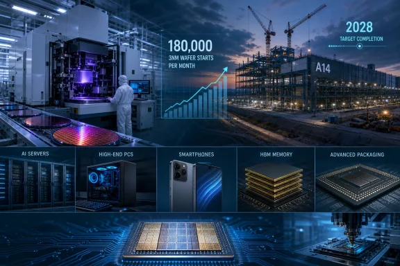
The distinction is more than semantic. The 180,000 figure began as a supply-chain estimate for end-2026 capacity, reported by Taiwan’s Economic Daily News and then repeated by TrendForce in April. The newer early-fourth-quarter timetable appears to come from another Economic Daily News report cited by Wedbush analyst Matt Bryson, who characterized it as information that would be positive if accurate. TSMC has confirmed it is converting 5nm lines in Taiwan to 3nm and adding worldwide N3 capacity, but it has not publicly confirmed either the 180,000 figure or the October-to-December timing.
The Taichung construction report is similarly narrower than the “1.4nm factory beats schedule” framing suggests. Tom’s Hardware Italy reported in July that the first A14 building could be completed by April 2027, followed by pilot production in the third quarter. TSMC’s own July earnings materials and its June annual meeting record still describe A14 development as proceeding to plan, with risk production in 2027 and volume production scheduled for 2028. There is no company announcement moving that production date forward.
For Windows users, PC builders and IT buyers, the immediate takeaway is that the AI supply chain may gain some breathing room in 2027, but it is premature to treat this as a broad end to accelerator shortages or an imminent drop in hardware prices. More leading-edge wafers help only after customers receive their allocated dies, pair them with HBM memory and get them through advanced packaging.
The 3nm acceleration is a supply-chain report, not a TSMC production commitment
TrendForce’s April report said TSMC’s Taiwan 3nm capacity had been expected to reach 150,000 wafers per month by the end of 2026 and was instead projected at 180,000. It explicitly attributed those figures to Economic Daily News supply-chain sources, rather than to TSMC. That report also placed the 180,000 target at year-end, not early in the fourth quarter.
The newer version of the story says TSMC was already near 150,000 3nm wafer starts per month in the first half of 2026 and could reach 180,000 at the start of Q4, two to three months ahead of market expectations. That is plausible in the context of TSMC’s confirmed expansion plans, but it remains an estimate based on unnamed sources. Bryson’s note did not independently validate the number; it assessed the implications of the report.
TSMC has nonetheless put important facts on the record. Chairman C.C. Wei said in April that the company is building new 3nm capacity in southern Taiwan and converting existing Taiwanese 5nm capacity to 3nm. TSMC also expects its second Arizona fab to begin 3nm volume production in the second half of 2027 and its second Kumamoto fab in Japan to use 3nm from 2028.
That conversion work explains why an earlier ramp is credible. It is faster to refit capacity within an existing advanced-node fab than to construct, qualify and staff an entirely new facility. But conversion capacity is not free capacity: the company is reallocating tools, floor space and engineering attention that could otherwise support 5nm-family output. The practical result is a shifting mix inside TSMC’s factories, rather than 30,000 additional wafers appearing from nowhere.
TSMC’s latest reported financial mix shows why the company is willing to make that trade. In the quarter ended June 30, 2026, 3nm accounted for 30% of its wafer revenue and 5nm accounted for 33%, while 2nm had already reached 3%. Leading nodes at 7nm and below collectively represented 77% of wafer revenue. N3 is no longer a niche leading-edge process reserved primarily for phones; it is one of TSMC’s central revenue engines.
Extra wafers do not translate directly into more Windows AI hardware
The submitted report treats 180,000 monthly wafer starts as if they translate directly into tens of millions of finished AI chips. They do not. A wafer start is the beginning of a long manufacturing flow, and it says nothing by itself about die size, yields, customer allocations, packaging capacity, HBM availability or product mix.
An N3 wafer used for a smartphone processor can yield dramatically more sellable dies than one used for a very large compute die. Many server accelerators also use chiplets built on different nodes, and their final availability can be governed by the supply of HBM stacks, substrates, interposers and packaging slots rather than by logic-wafer starts. A 20% rise in wafer starts therefore cannot be converted honestly into a fixed number of GPUs, NPUs or AI servers.
The customer mix also matters. Nvidia, AMD, Broadcom and Apple all compete for advanced TSMC capacity, while hyperscalers are expanding demand for custom ASICs. A larger N3 allocation may support graphics processors, data-center CPUs, networking silicon, laptop SoCs, custom AI accelerators or products that never reach a Windows device at all.
For organizations planning Windows AI PCs or GPU-backed workloads, the likely benefit is indirect. Greater 3nm supply can reduce the risk that one constrained customer segment consumes all available leading-node production, but it does not guarantee better availability of Nvidia RTX-class GPUs, AMD Instinct accelerators, Ryzen AI processors or cloud GPU instances. Those products are allocated under long-term contracts and arrive on their own qualification and launch schedules.
TSMC’s expansion is therefore best read as a positive sign for 2027 supply resilience, not as evidence that enterprise buyers should delay purchases expecting a near-term price reset. The silicon shortage can ease for one product category while packaging, memory or board-level power delivery remains tight somewhere else in the same system.
The packaging bottleneck may be changing faster than the wafer story
The strongest part of TSMC’s current investment case is not simply that it can print more advanced logic. It is that AI chips increasingly need advanced packaging to combine large logic die, memory stacks and chiplets into a usable accelerator module. On that point, the submitted report’s claim that CoWoS will remain a major binding constraint through year-end is already in tension with TSMC’s public messaging.
At TSMC’s April technology symposium, senior vice president Kevin Zhang said the company’s CoWoS capacity had grown enough to address customer demand “at this point.” That does not mean every package type, customer configuration or HBM combination is unconstrained. It does mean the company is signaling a more nuanced picture than a blanket packaging shortage.
TSMC is spending accordingly. It raised 2026 capital-expenditure guidance in July to $60 billion to $64 billion, up from $52 billion to $56 billion, and said its 2nm ramp and overseas expansion would weigh on margins. The scale of that spending supports additional capacity, but it also explains why the company has little incentive to turn a supply improvement into cheap wafers for customers.
The commercial consequence is straightforward: capacity additions may prevent the AI market from becoming even more supply-starved, while not eliminating TSMC’s pricing power. TSMC has not publicly announced the specific 3nm price increases claimed in the submitted report. Reports of 15% N3 increases in the second half of 2026 remain supply-chain reporting, not a published company price list.
A14 construction progress does not change the 2028 node race
The A14 part of the story is important, but the record supports a more restrained conclusion. TSMC announced A14 in April 2025 as its second-generation nanosheet process, promising up to 15% higher speed at the same power or up to 30% lower power at the same speed compared with N2, alongside more than 20% logic-density improvement. At its 2026 symposium, TSMC added A13 and A12 derivatives scheduled for 2029.
TSMC has also been consistent that A14, A13 and A12 do not require High-NA EUV in their initial forms. Zhang said in April that TSMC can continue using current EUV systems for A14 and A13 rather than moving to High-NA tools, which he called very expensive. That is a cost and manufacturing-complexity decision, not proof that TSMC has solved every future scaling problem without High-NA lithography.
Intel is taking a different route. Its public filings say Intel 14A is being designed to potentially incorporate High-NA EUV in high-volume logic manufacturing, and CEO Lip-Bu Tan said in July that Intel expects 14A risk production for internal products in the second half of 2027 and has committed to a high-volume ramp in 2028. The two companies are therefore still targeting broadly overlapping production windows, not the 12-to-18-month TSMC lead asserted in the submitted report.
Intel’s own annual filing adds a material commercial caveat: Intel 14A needs external wafer volumes to reach efficient economics, and the company has said it may pause or discontinue next-generation leading-edge development if it cannot secure a significant external customer. TSMC does not face that same customer-volume problem; its advanced-node business already serves a much deeper pool of fabless chip designers.
That is the real competitive advantage visible in the current reports. TSMC is adding N3 capacity while N2 ramps and while A14 remains on schedule, all with customers already filling the factory pipeline. The A14 building’s reported early completion would reduce construction risk, but until TSMC changes its own 2028 production guidance, it should be treated as execution progress rather than a roadmap acceleration.
TSMC’s next hard checkpoint is its third-quarter results and 2027 capital plan. If management publicly confirms an early-Q4 180,000-wafer N3 run rate, the industry will have a stronger basis to revise supply forecasts; until then, the number remains a well-sourced report, not a company commitment.