

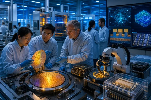
For Windows users and IT professionals, this is one step upstream of the products they deploy: EPIC is intended to shorten the development cycle for the materials, transistor structures, memory technologies and advanced packaging that determine how much performance—and how much power—future AI PCs, servers and accelerators can deliver. It does not announce a new processor, a Windows hardware feature, a foundry commitment, or a chip production program. It is a research-access agreement around Applied’s equipment and process-integration work.
The larger news is that Applied is filling out a deliberately broad pre-production consortium before the facility itself begins operations. Berkeley’s entry confirms that EPIC is being built as a place where equipment supplier, chip designer, chipmaker and university researchers can work on the same manufacturing problems earlier than they normally could.
Berkeley joins a center that is still not open
Applied’s release says the EPIC—Equipment and Process Innovation and Commercialization—Center is on track to become operational in 2026. That language deserves closer reading, because Applied’s own published timetable has moved.
When the company announced the project in May 2023, it said the Silicon Valley center was expected to be completed in early 2026. In May 2026, Applied described the site as expected to be “operationally ready this year.” Its 2025 Impact Report, published last month, offers the clearest current window: the company says EPIC is on track to begin operations in late 2026.
So Berkeley is joining a program that has partners and planned research tracks, but not yet a publicly confirmed operating cleanroom. The August 11 announcement does not give an opening date, state when Berkeley personnel will begin work there, identify a first project, or specify how much tool access the university will receive.
That is a material distinction. A university agreement can establish research priorities, staffing and legal frameworks before equipment is commissioned, but it does not mean Berkeley researchers are already running experimental wafers at the site. Applied’s claim is about a forthcoming collaborative environment; the practical test will begin when the facility is operating and partners disclose actual technical programs or results.
The value is process integration, not a campus lab upgrade
Berkeley is not short of semiconductor expertise. Its historical role includes work associated with SPICE circuit simulation and FinFET transistor design, the latter becoming fundamental to leading-edge logic manufacturing for much of the past decade. Applied’s own 2023 EPIC materials also included a Berkeley engineering dean’s endorsement, indicating the relationship was expected years before this week’s formal collaborator announcement.
What EPIC can add is access to the difficult middle ground between a laboratory result and a manufacturable technology. A material can look promising in a university environment yet fail when it must be deposited uniformly across wafers, patterned around fragile three-dimensional structures, cleaned without contamination, measured at production-relevant tolerances, and integrated with numerous other process steps. At modern nodes, an improvement to one layer can create yield, reliability or variability problems somewhere else in the stack.
Applied describes EPIC as a shared environment for advanced materials, device technologies, process integration and equipment development. Its May announcements with TSMC and three other universities use nearly identical language: academic teams would work alongside Applied scientists and engineers on research meant to reach commercial manufacturing faster.
That framing tells readers what Berkeley is—and is not—signing up for. This is closer to lab-to-fab translational research than unrestricted academic experimentation. Applied operates the tools, owns major parts of the equipment and process expertise, and sells to the manufacturers that would eventually industrialize successful work. Berkeley’s contribution is likely to be its research talent and new technical concepts; Applied’s is the ability to test whether those concepts survive real manufacturing constraints.
EPIC’s partner list gives Applied earlier visibility into the roadmap
The partner lineup reveals why Applied has put so much money behind the project. TSMC is collaborating at EPIC on materials engineering, equipment innovation and process-integration technologies for future logic scaling. Samsung joined to work on advanced node scaling, future memory architectures and extreme 3D integration. Applied’s university agreements emphasize advanced materials, novel devices, chip architecture inflections and AI-oriented energy efficiency.
Those are not separate buckets in a contemporary AI system. Logic transistors, high-bandwidth memory, wafer-level interconnects and advanced packaging increasingly have to be co-designed. A server-class accelerator may be constrained less by nominal transistor density than by memory bandwidth, heat, yield, interconnect density, power delivery or package reliability. The same applies, on a smaller power budget, to the neural-processing hardware entering PCs.
Applied said in its TSMC announcement that EPIC will give it greater “multi-node visibility” to guide its research investments. In plain terms, the equipment supplier gains earlier insight into the problems its customers expect at successive process generations. That is commercially valuable. It can help Applied decide which deposition, etch, inspection, metrology, materials and integration tools to develop before a customer is ready to purchase them at volume.
For Berkeley, proximity to that process could make research more relevant and give students experience with manufacturing-grade work. For Applied, the arrangement expands its funnel of ideas and potential engineers while bringing university research into a setting shaped by its product and customer roadmaps.
The announcement is therefore more consequential for Applied’s R&D model than for Berkeley’s existing reputation. Berkeley was already part of Applied’s orbit: the company cited previous collaboration through the Berkeley Emerging Technologies Research Center and CITRIS, plus shared laboratory space and campus recruiting. The new agreement appears to formalize and concentrate that relationship at the company’s flagship R&D site.
The $5 billion number needs context
Applied now refers to EPIC as a roughly $5 billion center and the largest U.S. investment in advanced semiconductor-equipment R&D. IEEE Spectrum has similarly described the initiative as a roughly $5 billion commitment, while Applied’s own materials say the spending is expected to scale toward that level as customer projects begin.
But the original 2023 announcement put the company’s planned gross incremental capital investment at up to $4 billion over seven years, contingent in part on CHIPS Act incentives, and projected more than $25 billion in company R&D investment through the center in its first decade. Those are different measures: capital construction and equipment spending, versus the much broader R&D activity expected to flow through the site over time.
Readers should not treat the $5 billion figure as a fixed, fully spent facility cost. Applied’s own May 2026 TSMC release says capital spending is expected to scale “over time” as customer projects commence. The company also has not disclosed the financial terms of the Berkeley collaboration, whether public funds are involved, or the allocation of cleanroom capacity among universities, chipmakers and other partners.
The intellectual-property details are missing as well. That is not a minor administrative matter in a shared semiconductor research center. Researchers need clarity on publication review, ownership of inventions, licensing rights, data access and the boundary between pre-competitive research and work that could become a supplier’s proprietary advantage. Neither Applied’s announcement nor the version carried by The Manila Times spells out those terms.
What this means for the AI hardware pipeline
Applied has consistently presented EPIC as an answer to a basic semiconductor problem: the time between identifying a promising material or structure and proving that it can work in high-volume manufacturing has become too long and expensive for isolated research teams. The company says its model can remove years from materials-development cycles. That is a vendor projection, not a demonstrated result; EPIC has yet to produce a publicly documented commercial breakthrough because its Silicon Valley facility has not opened.
Still, the structure is logical. Chip fabrication has become dependent on interactions between materials suppliers, tool vendors, foundries, memory makers, designers and packaging specialists. A university can invent an enabling material or device, but it cannot by itself establish the process window needed for commercial yield on state-of-the-art equipment. Conversely, a tool supplier can optimize a process faster when it understands the architectures customers and researchers are pursuing.
Berkeley’s participation strengthens Applied’s academic side after the company announced ASU, RPI and Stanford as inaugural university research partners in May. Its position in the same region as Applied’s Santa Clara operations also lowers the practical friction of collaboration: students and faculty can work with equipment and engineers without a multi-day trip to a distant research fab.
The immediate takeaway is restrained: UC Berkeley has joined the EPIC partner network, not a running production line. The actionable milestones will be the center’s late-2026 opening, the first named Berkeley programs, and evidence that a project has advanced beyond joint research into a qualified manufacturing process. Until then, the announcement is a strategically useful partnership—and another sign that Applied wants its equipment platform embedded in the research decisions that shape the next generation of AI silicon.