
That distinction gets blurred in Huawei Central’s comparison of the two efforts, which draws on claims from tipster FixedFocus. The comparison correctly identifies that both companies are pursuing denser vertical integration, but it treats Huawei’s Tau Law and Xiaomi’s wafer-on-wafer packaging as though they sit at the same engineering layer. They do not. One is a disclosed package-level design aimed at feeding an AI accelerator; the other is Huawei’s stated method for improving timing, layout density, and performance across devices, circuits, chips, and systems.
For PC and enterprise AI readers, the useful takeaway is straightforward: Xiaomi is attacking the memory wall for local models, while Huawei is trying to reduce the latency and wiring penalties that limit conventional planar silicon. Those approaches can overlap in a future product, but the evidence available on August 25 does not show that Huawei’s forthcoming Kirin design uses the same kind of wafer-on-wafer memory stack Xiaomi has announced.
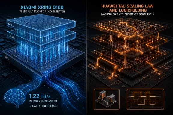 Xiaomi’s O100 puts memory directly beside AI compute
Xiaomi introduced the XRING O100 on August 24 as a 6 nm AI accelerator for running its MiMo large-language model on consumer devices. Reuters reported that Xiaomi has contracted TSMC for production of the O100, alongside the new XRING O3 smartphone processor and D100 automotive chip. The O100 is therefore not the successor handset SoC itself; it is a dedicated NPU-oriented part in Xiaomi’s wider XRING program.
The engineering detail that makes the O100 notable is its disclosed wafer-on-wafer arrangement. IT Home, reporting from Xiaomi’s chip technology event, said the design combines two DRAM wafers with one NPU compute wafer using hybrid bonding, creating a three-layer assembly. Xiaomi claims a 1.4-micron bonding pitch, 2.58 million bonding points, and memory bandwidth of 1.22 TB/s.
That architecture is designed around a practical constraint for local AI: model inference increasingly spends its time moving weights and activations rather than executing arithmetic. A large NPU can have impressive theoretical TOPS, but its real throughput falls if it repeatedly waits for external DRAM. Bringing memory into a vertically bonded structure creates many more, much shorter links between compute and storage than a conventional package can offer.
Xiaomi says its design uses face-to-face metal connections rather than the older approach of relying on larger micro-bumps and solder connections. The company’s claimed result is a high-bandwidth path intended to keep a 14-core NPU supplied with data while it runs MiMo locally. Xiaomi also says the O100 can reach 330 tokens per second for on-device inference, though that remains a vendor result rather than an independently published benchmark.
For Windows users, this design direction should sound familiar. Copilot+ PCs, workstation NPUs, discrete GPUs, and AI accelerators all face the same fundamental constraint: local AI performance depends as much on accessible memory bandwidth and capacity as on compute throughput. Xiaomi’s O100 does not create an immediate Windows hardware option, but it is a clear example of why future client AI chips may look less like a single flat processor and more like tightly integrated compute-and-memory systems.
Tau Law is Huawei’s design method, not a published package diagram
Huawei introduced the Tau Scaling Law at the IEEE International Symposium on Circuits and Systems in Shanghai on May 25, 2026. In Huawei’s own description, the proposal shifts emphasis away from geometric transistor shrinking alone and toward reducing the time constant, τ, of electronic systems. That means reducing the resistance, capacitance, wiring distance, and coordination overhead that delay useful work.
LogicFolding is one implementation under that framework. Huawei says it restructures circuit layouts to break the constraints of conventional planar design, shorten critical paths, reduce resistive and capacitive loads, and improve transistor density and circuit performance. Huawei describes Tau Law as extending from devices and circuits through chip-level workload-aware optimization and system-level interconnect design.
This is materially different from Xiaomi’s O100 disclosure. Xiaomi has described a particular physical stack: two DRAM layers bonded to an NPU wafer. Huawei has described an optimization approach in which logic blocks can be arranged across active layers to shorten the paths that matter most. Huawei’s public announcement does not provide a comparable bill of materials for the coming Kirin chip, such as the number of active tiers, memory layers, bonded die arrangement, package bandwidth, or thermal characteristics.
The Huawei Central article says Huawei’s forthcoming chips will use a “3D reconstructed design concept,” but Huawei’s official material is more cautious. It confirms that Kirin chips scheduled for fall 2026 will be the first to adopt LogicFolding, while leaving the commercial chip’s detailed physical implementation undisclosed. Until Huawei publishes a package breakdown or the chip reaches independent teardown and measurement, it is premature to equate LogicFolding directly with Xiaomi’s wafer-on-wafer DRAM stack.
The 41% figure is not a 41% performance increase
The comparison also repeats a potentially consequential numerical error. It says Huawei’s approach raises “overall chip performance” by 41% compared with a conventional 2D design. Huawei’s published Tau Law material instead describes a 41% reduction in power consumption at equivalent performance for its mobile SoC LogicFolding implementation.
Those are not interchangeable claims. A 41% performance gain would mean Huawei can finish a workload substantially faster under a comparable power limit. A 41% power reduction at the same performance means it can potentially hold existing performance while using less energy, producing less heat, or allocating saved power elsewhere in the chip. Both outcomes can be valuable, particularly in thin phones and compact AI hardware, but they affect product comparisons differently.
Huawei has also described density and clock improvements associated with its proposed Kirin 2026 implementation. Reporting by the South China Morning Post said Huawei’s updated paper claimed a roughly 55% transistor-density increase versus the Kirin 9030 Pro. Huawei’s own May announcement did not give the later detailed percentages, but it did say LogicFolding would be deployed first in the fall 2026 Kirin line and projected that high-end chips based on Tau Law could reach transistor densities equivalent to a 1.4 nm process by 2031.
Those are Huawei claims awaiting commercial validation. Density, clock speed, energy efficiency, sustained performance, yields, and thermals can move independently. A 3D structure that improves path length may also create harder heat-removal, power-delivery, and manufacturing-yield problems. Xiaomi faces similar issues in its memory stack; its public remarks acknowledge work to address wafer warping and breakage during high-temperature bonding.
Bandwidth versus timing is a useful dividing line
The cleanest comparison is not “which company has better 3D packaging?” It is what each company is trying to optimize first.
Xiaomi’s O100 design is explicitly bandwidth-led. Its bonded DRAM and NPU structure is meant to create a very wide, local memory path for model inference. If Xiaomi’s 1.22 TB/s claim holds in shipping hardware, it would make the O100 an unusually bandwidth-rich device-side accelerator for a consumer product. The trade-offs will be capacity, package cost, yield, power, and cooling, none of which Xiaomi has fully detailed.
Huawei’s Tau framework is latency- and efficiency-led. LogicFolding aims to shorten critical signal paths and improve the effective density of logic without relying solely on an advanced process node. The Tau proposal also extends beyond the physical chip, incorporating workload scheduling and system interconnects. That makes it conceptually broader than a packaging technology, but it also makes simple headline comparisons harder: an improvement attributed to Tau Law may involve architecture, software, routing, and system behavior rather than one bonded stack.
Huawei Central’s underlying point that neither approach can be declared the winner before shipping products are tested is sound. But the test will not be a single benchmark. Xiaomi needs to prove that its memory bandwidth translates into sustained local-model throughput in a practical thermal envelope. Huawei needs to show that LogicFolding delivers its claimed density, efficiency, and timing benefits in a mass-produced Kirin chip rather than in design data and roadmap projections.
For now, Xiaomi has disclosed the more concrete package-level product: a 6 nm NPU with vertically bonded DRAM intended to speed local AI. Huawei has disclosed the more ambitious design philosophy, with a first consumer implementation still ahead. The real comparison begins when Huawei’s fall 2026 Kirin device ships and both companies’ claims can be tested under sustained workloads rather than presentation slides.
