

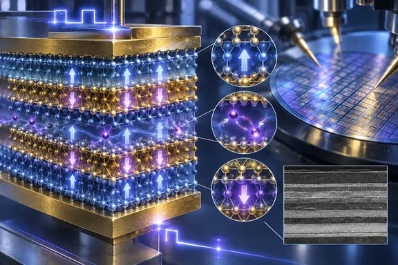
The important qualifier is that this is a materials-and-device endurance result, not a new RAM product or a replacement for the DRAM in PCs and servers. The team from Xidian University, City University of Hong Kong and Fudan University made a layered AlScN/aluminum nitride structure and paired it with an active recovery routine. That combination matters: the reported leap is not evidence that every AlScN memory cell can now survive 10 billion writes.
South China Morning Post independently reported the same core result and the collaboration behind it. The primary Science record confirms both the figure and the measurement threshold: the material retained a remanent polarization of at least 100 microcoulombs per square centimeter after more than (10^{10}) complete switching cycles. That is a stronger claim than merely detecting some residual ferroelectric behavior after a long stress test.
The endurance failure was traced to a moving defect
Ferroelectric memory stores a bit by reversing the direction of electrical polarization in a material. In a practical device, that offers an appealing combination: nonvolatile storage, potentially fast switching, and compatibility with semiconductor manufacturing methods. AlScN has attracted attention because it belongs to the wurtzite family of nitride materials and can be deposited in ways that fit more naturally with CMOS process flows than some older ferroelectric candidates.
But repeatedly forcing the polarization to reverse is punishing. The Science authors say conventional wurtzite ferroelectrics generally fail around (10^8), or 100 million, cycles. At that point, leakage current rises, dielectric breakdown becomes likely, and the material can no longer reliably retain or switch its polarization.
The team’s contribution is an explanation at the defect level. A nitrogen vacancy is exactly what it sounds like: a location in the crystal lattice where a nitrogen atom should be but is absent. Such vacancies are unavoidable to some degree in real deposited films. The researchers found that, during repeated switching, vacancies could cluster and migrate over longer distances, eventually forming conductive leakage paths through the material.
That is a useful advance beyond a generic “fatigue” label. The group’s earlier work, published in Science China Information Sciences in August, also identified nitrogen-vacancy-driven degradation in ferroelectric AlScN. The new paper turns that diagnosis into an endurance strategy: stop vacancies from collecting into the paths that lead to electrical failure.
The 100-fold gain came from two interventions
The sample that exceeded 10 billion cycles was not a plain AlScN film. It was an AlScN/aluminum nitride superlattice: thin AlN layers were inserted periodically into the AlScN material. Those AlN layers act as barriers that make it harder for nitrogen vacancies to move vertically through the film and join up with other defects.
The second intervention is easier to miss in headline coverage but is just as important. The researchers also used what the Science abstract calls a “dynamic recovery protocol.” In the public preprint corresponding to the study, the team describes periodically applying recovery pulses intended to return defects to more stable locations before the material crosses into catastrophic degradation.
In other words, the result is not simply “a better film survived 100 times longer.” It is a structural design combined with a cycling-management technique. For memory engineers, that shifts the question from whether a cell lasts under a continuous test to whether recovery operations can be incorporated into a useful array, controller and workload without turning endurance maintenance into a performance, energy or design-complexity penalty.
That does not weaken the materials result. It makes the engineering work ahead much clearer. A recovery pulse may be a reasonable background operation in some nonvolatile-memory designs, especially if it is infrequent and can be scheduled outside latency-sensitive writes. But it is an operational requirement that a commercial implementation would need to characterize, validate and expose to system designers.
The 10 billion figure has a temperature caveat
The headline number is real, but its test conditions deserve more attention than the coverage has received. In the authors’ June 2025 preprint, which carries the same title, author list and core AlScN/AlN superlattice approach as the final Science paper, the more than (10^{10})-cycle demonstration was conducted at 250 kelvin, about -23°C (-9°F). The paper also reported multi-billion-cycle behavior at 300 kelvin, roughly room temperature, but the more than 10-billion result was associated with the colder test.
That distinction is consequential. Data-center hardware, laptops and embedded systems are not normally designed to run their memory arrays at -23°C. Cryogenic or sub-ambient operation can be realistic in specialized research, sensing and high-performance environments, but it is not an ordinary deployment condition for server memory.
The Science abstract confirms the beyond-10-billion figure and the complete-switching criterion, but it does not state the test temperature, pulse amplitude, frequency, retention time or the array scale in the public abstract. TechRadar’s report also did not surface those conditions. Readers should therefore treat the result as a major reliability demonstration under a defined experimental regime rather than as a commercial endurance specification.
The authors’ preprint also indicates 100 kHz bipolar switching and electric fields in the multi-megavolt-per-centimeter range. Such fields are common in ferroelectric characterization, but they underline another unanswered product question: whether a scaled device can maintain its endurance, switching voltage and energy characteristics together after integration with access transistors, interconnects and dense arrays.
Why this still matters for future compute hardware
Nonvolatile memory that switches quickly and survives heavy rewriting could be valuable in several places where today’s hierarchy forces compromises. Conventional DRAM is fast but loses data without power. NAND flash retains data but is far slower and has much lower write endurance. Ferroelectric approaches aim to occupy part of the wide gap between them, potentially serving embedded nonvolatile memory, storage-class layers, or compute-in-memory designs where local data movement is a major energy cost.
AlScN has a particular appeal because nitrides already have a foothold in semiconductor fabrication and because the material’s large polarization can support dense cells. The research team argues that controlling vacancy topology could support “ultradense” ferroelectric memory. The key word is could: the work establishes a route to a more durable switching material, not a demonstrated high-capacity chip.
For AI hardware, that distinction is especially relevant. The bottleneck in many AI systems is moving weights and intermediate data between compute and memory, not merely performing arithmetic. Nonvolatile memory placed closer to logic is an active research direction because it could reduce that movement. Yet a laboratory capacitor or test structure must still become a manufacturable array with selectors, predictable variability, data retention, endurance distribution, error management and acceptable write energy.
A 10-billion-cycle cell would not automatically solve those system problems. It does remove one unusually stubborn objection to using wurtzite ferroelectrics at all: the previous tendency to fail near 100 million switches even when researchers wanted strong, full polarization reversal.
What has not yet been shown
The paper’s result should prompt careful interest rather than a rush to declare a new memory tier. There is no announced commercial process, foundry partner, memory density, product timetable or PC/server roadmap. Neither the primary abstract nor the reporting reviewed here establishes a packaged memory array with billions of independently addressable cells.
Several measurements would determine whether this becomes more than an endurance milestone:
- A practical device will need retention data after the same cycling and recovery regimes, rather than endurance data alone.
- Large arrays will need to show that the AlScN/AlN layering and recovery behavior remain consistent across wafers and across cells.
- Designers will need write-voltage, write-energy and latency numbers after integration with the circuitry required to select individual memory cells.
- Reliability testing will need to cover ordinary operating temperatures, thermal cycling and workload patterns rather than a single high-frequency switching experiment.
The immediate result is still substantial. Xidian University and its partners have moved wurtzite AlScN ferroelectrics from a roughly 100-million-cycle reliability barrier to a controlled experiment exceeding 10 billion complete writes, while identifying the physical failure mechanism that had been obscuring progress. The path to a deployable memory chip now runs through array-scale manufacturing and room-temperature validation, not through another search for the defect that causes the material to break.
References
- Chinese scientists achieve 10 billion writing cycles in major future memory endurance breakthrough that improves endurance by 100x TechRadar · 2026-09-16T22:10:00+00:00