

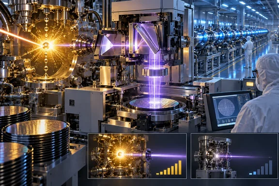
The key correction is that ASML has already demonstrated 1,000 watts. Its 2025 annual report says the company reached that milestone in April 2025, by lifting the tin-droplet firing rate from 60,000 to 100,000 plasma events per second and improving the laser and plasma recipe. What ASML has not announced is a commercial scanner shipping with a 1,000-watt source, a release date for one, or a customer qualification schedule.
That distinction changes the story for chipmakers and the PC industry. ASML is not choosing between a mature 1,000-watt plasma source and a theoretical accelerator. It is extending a source architecture that already operates in volume production, while FEL advocates still have to prove that a particle-accelerator installation can meet semiconductor-fab requirements for uptime, maintenance, contamination control, beam delivery, serviceability and cost.
ASML’s 1,000-watt milestone is a laboratory demonstration, not a product launch
ASML’s extreme ultraviolet systems create 13.5-nanometer light by firing high-power carbon-dioxide laser pulses at molten tin droplets. A preparatory pulse reshapes a droplet, then a stronger pulse turns it into a short-lived plasma that emits EUV radiation. The scanner’s collector optics capture a small fraction of that light and send it, through a vacuum-only optical path, to the rest of the lithography system.
This is an elaborate route to illumination, but it is one ASML and its suppliers have industrialized over decades. ASML says its latest commercial sources run at 60,000 droplets per second. The 1,000-watt demonstration raised that to 100,000 per second, a 67% increase in repetition rate, alongside higher laser capability and improved plasma operation.
ASML’s own description contains the material caveat missing from the more definitive headline: it said a commercial 1,000-watt source would take “some time.” The company did not attach a shipment year to that statement. Neither Reuters’ account of the JPMorgan meeting nor Tom’s Hardware’s report supplies a product model, field-installation plan, or evidence that a customer has qualified a 1,000-watt source in production.
The current production baseline is materially lower. ASML’s 2025 report lists the NXE:3800E at 230 wafers per hour under its cited test conditions, up from 220 wafers per hour for the preceding measurement. That system-level productivity comes from more than raw source power: dose requirements, resist behavior, mask and pellicle performance, overlay, wafer-stage speed, scanner availability and optical transmission all determine how many good wafers a fab can expose.
Higher source power matters because it can reduce exposure time and raise throughput, but watts at the source are not interchangeable with wafers at the end of a fab line. A 1,000-watt milestone validates headroom in ASML’s plasma roadmap. It does not establish a near-term doubling of commercial chip output.
Free-electron lasers move the hard problem outside the scanner
A free-electron laser offers a radically different proposition. Instead of repeatedly vaporizing tin inside each scanner’s source vessel, an FEL accelerates electrons and sends them through an undulator—an array of magnets that makes the electron beam oscillate and emit coherent light. In principle, the source can be tuned for EUV wavelengths, run at far higher average power and potentially serve multiple scanners from one central facility.
Those are substantial theoretical advantages. FEL developers argue that removing tin plasma from the source eliminates debris-management problems and could provide a path to shorter wavelengths beyond today’s 13.5-nanometer EUV. xLight, one of the companies pursuing the approach, says its design could connect to existing ASML scanners and provide higher EUV power from a shared source.
But an FEL does not make complexity disappear. It relocates it into a facility-scale machine: electron injectors, accelerator structures, high-precision beam control, an undulator, vacuum infrastructure, shielding, high-power optics and a distribution network that must carry EUV to multiple lithography tools. Each component has to operate continuously in an environment where unplanned downtime is extraordinarily expensive.
The central technical challenge is therefore not simply generating bright EUV. Scientific FELs have generated powerful short-wavelength radiation for years. The commercial challenge is delivering that radiation with fab-grade availability and with predictable maintenance, stable dose control, acceptable electricity use, compact enough physical infrastructure and economics that beat continued improvements to an installed LPP base.
ASML’s reported position reflects that engineering reality. A chipmaker already has an ASML scanner fleet, process recipes, service arrangements, contamination controls and trained operations teams built around plasma sources. Replacing the light source with a facility-scale accelerator is a systems-integration project, not a component swap, even if an FEL developer describes it as backward-compatible.
xLight has public funding and a prototype target, but not a production tool
FEL development is no longer a purely academic alternative. On June 2, the U.S. Department of Commerce and the National Institute of Standards and Technology finalized $150 million in CHIPS Act incentives for xLight to construct and demonstrate an FEL prototype at the Albany NanoTech Complex in New York. The award is an official federal commitment to test the premise that accelerator-driven EUV can become a manufacturing light source.
The Commerce announcement is important precisely because of what it says and does not say. It funds construction and demonstration of a first-of-its-kind prototype; it does not certify an FEL as production-ready, guarantee integration into ASML equipment, or establish an operating cost per wafer. Manufacturing Dive reported that xLight aims to use the Albany prototype in 2028, placing the first meaningful public test of the concept well after ASML’s 2025 source-power demonstration.
xLight’s public claims are ambitious. It says an FEL could provide as much as four times the EUV power of present laser-produced plasma sources and improve fab economics. Those remain company claims rather than independently demonstrated fab results. The federal award corroborates that the project has been funded for a prototype; it does not corroborate the promised power multiplier, per-wafer savings, multi-tool distribution architecture, or reliability level.
That is why describing ASML as having “snubbed” FEL technology risks overstating the evidence. Reuters reported JPMorgan’s interpretation after a CFO meeting, not an ASML product announcement declaring an industry-wide rejection of free-electron lasers. ASML has a credible reason to prioritize its LPP roadmap, and it publicly says LPP was originally selected partly for lower maintenance downtime and scalability. But no public record in the reporting reviewed establishes that ASML has permanently ruled out every accelerator-based source architecture.
The immediate race is throughput, not a change in EUV physics
ASML’s business priority is to supply more EUV systems and make each one process more wafers. Reuters reported that the company is examining ways to produce more than 110 EUV tools in 2028 to meet AI-driven demand. That manufacturing-scale objective makes an incremental source upgrade more attractive than a wholesale change in light-source infrastructure.
For Intel, TSMC, Samsung and the companies building PC processors, AI accelerators and high-bandwidth memory, the near-term implication is straightforward: plan around ASML’s laser-produced-plasma roadmap. The relevant improvements will arrive as scanner productivity upgrades and new platform generations, not as an abrupt conversion of fabs into accelerator halls.
The longer-term implication is more competitive. FEL research attacks one of EUV lithography’s persistent bottlenecks: the amount of usable light that can be delivered to the wafer. If xLight or another developer demonstrates a source with high power, high uptime and viable distribution economics, it could give fabs an alternative route to higher throughput and future shorter-wavelength lithography. Yet that remains a future manufacturing qualification problem, not a present replacement for ASML’s source technology.
ASML has already crossed 1,000 watts in a demonstration and is working to turn the result into commercial equipment. xLight’s federally backed FEL prototype is targeted for 2028. Until the latter produces repeatable fab-grade performance—and demonstrates that its central accelerator and beam-delivery system can be operated more economically than many proven plasma sources—the practical EUV roadmap for advanced chips remains the one that fires lasers at tin droplets 100,000 times a second.
References
- ASML snubs Elon Musk-backed particle accelerator chipmaking tech — firm doubles down on 1,000W laser-produced plasma systems for chipmaking tools Tom's Hardware · 2026-09-18T11:00:00+00:00