

The argument holds up better than most "the future of GPUs is…" takes. It also has more caveats than the headline suggests. Here is what the evidence supports, and where you should stay skeptical.
The case against "software will save us"
Butler gives DLSS a lot of credit. He calls NVIDIA's choice to spend die area on dedicated AI hardware "visionary." He says DLSS largely fixed the problem of running a high-resolution panel at a lower internal resolution without the blurry results old scalers produced. He also gives smaller credit to AMD's FSR and Intel's XeSS.
He also accepts part of a common complaint: some developers may be using DLSS as a crutch to cover weak generation-to-generation gains in raw GPU power. His main point is that upscaling can't remove the physical limits on making faster chips. Software can make better use of the silicon you have. It can't give you more silicon.
That framing works because the two approaches do different jobs. Reconstruction and frame generation raise the number of frames you see on screen. The hardware decides how much compute and memory bandwidth exists in the first place. A generated frame isn't free native rendering. It also doesn't respond like a native frame in every game and every setup.
Section summary: DLSS is a multiplier, not a replacement for compute. To get more real compute, chipmakers have to get past manufacturing limits.
The monolithic wall
Butler sums up the hardware problem in three constraints:
- Transistor scaling: Current lithography is approaching its practical limits, which is the same wall CPUs face.
- Die size: Each wafer has a fixed area. Bigger chips mean fewer chips per wafer and a higher cost per chip. Butler also cites a hard reticle limit of roughly 26 × 33 mm on how big a single exposed die can be. That figure is his. I haven't verified it here.
- Yield: Defective dies get thrown out, and their cost lands on the good ones. Big dies are hit harder, which is why makers often sell partly defective top-end dies as lower-tier cards with some compute units disabled.
Wafer-scale chips do exist. Butler rightly notes that nobody should expect a gaming GPU the size of a dinner plate.
Section summary: Large monolithic GPUs are one big, expensive bet per die. If you scale them up, you get worse yields and higher prices.
Chiplets: the "forbidden LEGO"
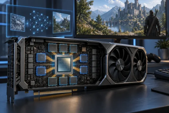
The alternative is to build the processor from several smaller dies. Small dies yield better and cost less each. AMD used this approach to great effect in Ryzen and EPYC CPUs. Intel took a while to follow.
The difficult part is the connections between dies. Even small communication bottlenecks can erase the gains. GPUs are much harder to split than CPUs. Custom PC explained it this way when RDNA 3 launched: inter-die communication is a significantly greater difficulty when dealing with the thousands of internal connections of a GPU, compared to the hundreds required within a chiplet-based CPU design.
Butler also points to Apple Silicon. In some of Apple's chips, apps see multiple GPU blocks as one logical GPU.
What RDNA 3 actually split up
Butler says RDNA 3 uses chiplets "for components like cache units." That's correct, and the details matter. AMD's launch materials describe a new 5nm 306mm² Graphics Compute Die (GCD) with up to 96 compute units that provide the core GPU functionality, alongside six of the new 6nm Memory Cache Die (MCD) at 37.5mm², each with up to 16MB of second-generation AMD Infinity Cache technology.
So Navi 31 isn't six compute chiplets working together. It is one compute die surrounded by memory and cache dies. HWCooling's coverage adds that these chiplets contain memory subsystem components – notably a GDDR6 memory controller with a total width of 64 bits per chiplet and a 16MB Infinity Cache block. This is the "put the leading-edge node only where it pays off" strategy Butler describes. The compute die uses 5nm, and the cache and memory-interface dies use the cheaper 6nm process.
AMD connected the dies with Infinity Links and high-performance fanout packaging, claiming up to 5.3TB/s of bandwidth. That number is a vendor specification, not a game benchmark.
Two details show the tradeoffs Butler only touches on:
- Latency costs. According to Custom PC, one downside of Infinity Fanout Links is an increase in latency over using an on-die cache. AMD's fix was to crank up the clock speed of the Infinity Fabric by 43 percent to achieve the same overall cache latency as on Navi 21. In other words, moving cache off the main die took extra engineering just to match the old latency.
- Not the whole RDNA 3 lineup used chiplets. Tom's Hardware's spec breakdown lists the RX 7900 and 7800/7700 cards on TSMC N5 plus N6. The budget RX 7600 (Navi 33) is a single 204 mm² die on TSMC N6 alone. Even AMD's first chiplet gaming generation used a monolithic die at the low end, where a single small die costs less than packaging several.
Section summary: RDNA 3 split compute from cache and memory interfaces across process nodes, at a cost in latency and packaging. It didn't build a GPU out of interchangeable compute tiles.
Data-center GPUs show more, with conditions
Butler cites AMD's Instinct MI300X as an example of going further. AMD's ROCm engineering blog confirms the layout: one MI300X has eight Accelerator Complex Dies (XCDs) and four I/O dies. Each pair of XCDs is 3D-stacked on an I/O die, and there are eight HBM stacks, two per I/O die.
That same AMD blog also complicates the idea that software always sees "one GPU":
- In the default SPX mode, the
amd-smiutility shows all eight XCDs as a single logical device. Work is spread round-robin across them, and the programmer doesn't control which XCD gets what. - In CPX mode, each XCD appears as its own logical GPU. An eight-MI300X server then reports 64 GPUs.
- The NPS4 memory mode, which keeps each XCD close to its local HBM, works only with CPX. In AMD's own stream microbenchmark, CPX/NPS4 reached about 4,210 GB/s of total bandwidth, compared with roughly 4,010 GB/s in the more unified modes. In an FP16 matrix-multiply test, the CPX modes delivered 10–15% more total throughput than SPX.
AMD says plainly that these simple kernels don't represent peak performance. It also says real applications that have to communicate across memory partitions may not see the same gains. The lesson for consumer GPUs: a multi-die package can be presented as one device, but getting the best performance often depends on the software knowing where memory lives. Games aren't written that way today.
NVIDIA's Blackwell is Butler's other example. NVIDIA's architecture page says Blackwell data-center products use two reticle-limited dies joined by a 10 TB/s chip-to-chip interconnect and presented as one GPU, with 208 billion transistors on a custom TSMC 4NP process. Butler notes that NVIDIA didn't use this two-die design for consumer cards and calls the RTX 5090 monolithic. He also says AMD went back to a monolithic design for RDNA 4. I couldn't independently confirm either company's reasons, so treat any explanation of why they chose this as speculation.
Section summary: Multi-die GPUs are already shipping in data centers. Their "single GPU" behavior depends on operating modes and how aware the software is of the layout.
Analysis: an option, not a promise
Butler's core claim holds up: chiplet GPUs aren't a distant idea, they are already here. His conclusion is also measured. He says chiplets don't guarantee cheaper GPUs, because advanced packaging is expensive. He hopes that the money AI is pouring into packaging research eventually reaches gaming hardware.
Here is where I'd push back:
- The consumer evidence is mixed. The best-known chiplet gaming GPU split off cache rather than compute. Both AMD and NVIDIA have stuck with monolithic dies for at least their latest consumer designs, according to Butler's own account. If chiplets were clearly better for gaming right now, you'd expect them to have spread.
- Gaming is unforgiving about latency. Data-center work like matrix math tolerates partitioning. A game frame with tightly coupled shading, ray tracing, and post-processing steps doesn't split as easily. The MI300X results show how much tuning a multi-die package needs.
- Hardware and DLSS work together. The likely future isn't chiplets instead of neural rendering. It's chiplets (or their successors) providing more compute, and neural rendering making each unit of it go further.
So is DLSS still the future? Partly. Raw hardware scaling isn't dead. It has just become a packaging problem as much as a lithography problem.
If you're shopping for a GPU now, none of this changes today's buying decision. Pick cards based on measured performance in the games you play, not on whether the die is monolithic. For people who follow the industry, the things to watch are whether a future consumer GPU splits compute across dies, and whether games can run on one without the latency penalties that have kept gaming GPUs mostly monolithic. If you want to dig deeper, look at our GPU hardware and PC gaming performance threads.
References
- I was wrong: DLSS isn't the future of GPUs, but this is How-To Geek · 2026-10-01T18:30:14+00:00
- NVIDIA Blackwell: GPU Architecture for Generative AI & HPC | NVIDIA nvidia.com
- AMD RDNA 3 details: architecture changes, AI acceleration, DP 2.1 - HWCooling.net hwcooling.net