

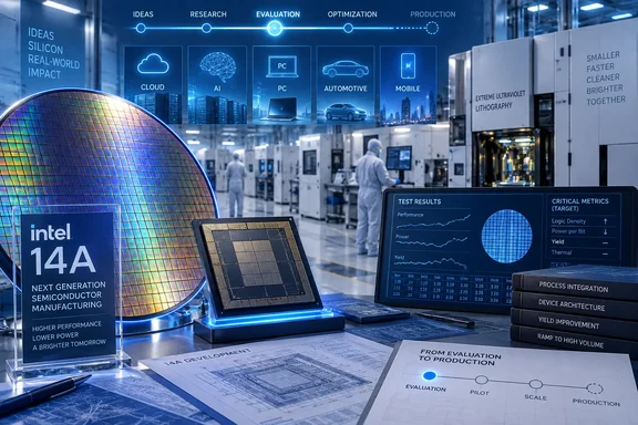
For Windows and enterprise IT readers, the practical significance is less about whether a given hyperscaler has run early 14A data through its engineering teams and more about what happens next: a customer must commit a real chip design, reserve capacity, and ultimately bring a product to market. Intel needs those commitments to make its expensive leading-edge foundry expansion economically viable. The company has already said the scale and pace of its manufacturing build-out will depend on committed demand for 14A from both Intel’s own product roadmap and external design wins.
The distinction is material. Evaluation is an early, normal stage in semiconductor procurement; it can involve process design kits, library data, manufacturing rules, simulation, and discussions about capacity. A production agreement requires a far more consequential decision: placing a future product’s schedule, yield targets, supply chain and profit margins in Intel’s hands.
Intel confirms external interest, but not the names
The named-company list reported by Wccftech remains unverified outside its account of Piper Sandler’s research note. Neither Intel nor Amazon, Apple, AMD, Google, Tesla, Microsoft, Nvidia or Qualcomm has publicly confirmed a 14A evaluation in response to this report. That does not disprove the list—chip-foundry evaluations are typically covered by non-disclosure agreements—but it defines the record as it stands.
Intel’s second-quarter 2026 filing provides the firmer baseline. It says the company committed during the quarter to finish Intel 14A development, has future Intel products designed for the node, and has made progress toward performance and design milestones for potential significant customers. Intel also said it intends to accelerate several manufacturing expansion projects, but tied their ultimate size and timing to committed 14A demand.
That language is more meaningful than a vague assertion of customer interest, because it indicates prospective customers are far enough along to influence Intel’s technical milestones. It still does not establish that any outside company has selected Intel 14A for a production chip. In foundry terms, the announcement readers should watch for is a design win, a long-term wafer agreement, or a customer naming Intel in connection with a specific processor, accelerator, mobile SoC or custom silicon program.
Intel has also said it expects early design commitments to emerge in the second half of 2026 and expand through the first half of 2027. That makes the next several quarters the window in which today’s evaluation claims either turn into booked business or remain an encouraging but preliminary pipeline.
The 14A schedule is more specific than the report suggests
Intel’s public schedule is narrower than the submitted report’s claim of risk production in the second quarter of 2027 and volume production by the first quarter of 2028. In its July 2026 earnings materials, Intel said 14A risk production for its internal products is planned for the second half of 2027, followed by a high-volume ramp in 2028.
Those are not interchangeable milestones. Risk production is the period in which a fab begins manufacturing real customer-like wafers while yield, defect reduction, tooling and process controls are still being proven. High-volume manufacturing is the stage that determines whether Intel can supply commercial products at a cost and volume customers can accept.
Intel has committed to a 2028 high-volume ramp, but has not publicly committed to a first-quarter 2028 start. Readers should treat a Q1 2028 date as reporting attributed to Wccftech rather than as Intel guidance. The official record leaves Intel room within 2028, and a broad annual ramp target is a meaningful difference for companies planning chips that may take years from process selection to retail or data-center deployment.
Intel CFO David Zinsner has said the 14A defect-density curve is progressing ahead of the company’s target curve, a data point also reported by Tom’s Hardware after his Deutsche Bank technology-conference remarks. Defect density is a useful manufacturing indicator: fewer defects per unit wafer area generally improve the number of usable chips produced from each wafer. Yet it is not a yield guarantee, nor does it settle questions around performance, power, design enablement, packaging, customer-specific IP, and capacity.
The process itself is intended to build on Intel’s RibbonFET gate-all-around transistor architecture and introduce PowerDirect backside power delivery. Intel says the approach should improve transistor density and power delivery by moving power routing to the wafer’s backside, leaving the front side more available for signals. The competitive question is whether Intel can turn those architectural claims into repeatable, high-volume yields on schedules that fit customers’ product roadmaps.
Intel’s own products lower the all-or-nothing risk
One critical change in Intel’s position is that 14A is no longer presented as an external-foundry gamble alone. The company has said a number of future Intel products are designed to use the node, and that internal demand helped support its decision to fully commit to the 2028 ramp.
That matters because Intel can use its own CPU, data-center and accelerator roadmaps to qualify process technology and generate baseline wafer demand before an outside customer’s product arrives. For PC buyers, enterprise administrators and OEMs, an internally used 14A node could eventually affect the supply, cost and cadence of Intel’s client and server chips even if the company’s biggest external prospects do not all convert into customers.
It does not remove the foundry business case. Intel’s own disclosures acknowledge that leading-edge nodes require enormous capital investment and that economic efficiency depends on wafer volumes beyond what it expects from internal products. Outside customers remain central to whether 14A becomes a profitable foundry platform rather than merely the manufacturing base for Intel’s next generation of chips.
The reported customer roster also illustrates why a confirmed win would matter. Amazon, Google, Microsoft and Tesla develop custom silicon for cloud infrastructure and AI workloads; Apple and Qualcomm have major mobile chip programs; AMD and Nvidia design high-performance computing and AI products. Any one of those customers could bring substantial technical validation, but each also has entrenched supply relationships and its own packaging, IP, performance and geographic requirements. Interest from all eight does not imply that all eight have compatible needs, or that Intel has capacity for all of them.
The $20 billion stock sale supports capacity, not a hidden customer announcement
Intel’s August equity offering added another reason investors are connecting 14A progress with fab expansion. The company initially proposed a $15 billion common-stock sale, then upsized it to $20 billion, producing approximately $19.7 billion in net proceeds before any additional underwriter shares. Intel stated that the money was intended to support growth opportunities, maintain its balance sheet and preserve its investment-grade credit commitment.
The filing did not identify a 14A anchor customer, allocate the money to Fab 62, or disclose a specific capacity purchase by an outside chip designer. Claims that the capital raise itself proves a signed 14A customer are therefore an inference, not a disclosed fact.
The more defensible reading is that Intel has chosen to preserve financial flexibility while it commits to 14A development and prepares for a capital-intensive 2028 ramp. That choice is consistent with growing confidence in the node and potential customer demand, but the company’s own filings make clear that the largest capacity decisions remain conditional on binding commitments.
Intel is trying to solve two problems at once: demonstrate that it can execute on a leading-edge process after years of manufacturing setbacks, and prove that external customers will trust it with products that have historically gone to TSMC or Samsung. The first problem is increasingly visible through defect and schedule disclosures. The second remains largely confidential until a customer names a program.
What Microsoft and other buyers would need to decide
For Microsoft, an evaluation of Intel 14A—if the Piper Sandler account is accurate—would most plausibly concern future custom data-center silicon rather than an immediate change to Windows PCs or Surface hardware. Microsoft already operates large Azure infrastructure and has publicly invested in its own cloud chips, so keeping another U.S.-based advanced manufacturing option under review would be commercially rational. But Microsoft has not announced an Intel 14A contract, a chip program, expected volumes or a deployment date.
The same caution applies across the reported group. Foundry customers do not select a node solely because it looks technically competitive on a presentation slide. They need validated design tools, intellectual-property blocks, advanced packaging, predictable capacity, commercial terms and confidence that the supplier will still be competitive by the time a chip reaches market.
Intel’s next concrete checkpoint is the 14A process design kit update expected later this year, followed by the first disclosed design commitments across late 2026 and early 2027. Until an external customer confirms a product or wafer agreement, the headline is evidence of serious industry interest—not evidence that Intel has broken TSMC’s hold on the most valuable chip contracts.
References
- Intel’s 14A Process Is Currently Being Evaluated By Amazon, Apple, AMD, Google, Tesla, Microsoft, NVIDIA, And Qualcomm, According To Piper Sandler Wccftech · 2026-09-18T15:06:54+00:00