

What Intel actually patented
The patent is US 12,733,303 B2, "IC package with micro LEDs," assigned to Intel Corporation. According to the USPTO Official Gazette entry dated September 8, 2026, Intel filed application 17/903,126 on September 6, 2022. The application was first published as US 2024/0079530 A1 on March 7, 2024. The grant contains 14 claims, and all nine listed inventors are based in Arizona, in Gilbert, Chandler, Scottsdale, Tempe and Phoenix.
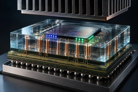
Claim 1 is the legal core. It describes an integrated-circuit package made up of:
- A semiconductor die with a micro-LED attached to it
- A glass substrate that at least partly embeds the die
- A TGV inside the glass that is electrically coupled to the die and touches it, supplying power to the micro-LED
- A package substrate coupled to that TGV
That is a package architecture. It isn't a shipping processor, a demonstrated production part or a working optical link. The 2022 filing date also explains the timing: this idea has been moving through the patent system for about four years.
Section summary: Intel owns a granted U.S. patent on a glass-core package with an embedded, LED-bearing die. Nothing in the record ties it to a product, model number or release window.
How the package is built
Tom's Hardware describes the main drawing like this. A glass substrate sits between two layers of package substrate, and a semiconductor die is partly embedded in the glass with its back surface exposed. The patent also allows the die to be fully embedded. The LEDs connect to the die either directly or through nanowires, and the TGVs carry power and signals through the glass.
Tom's Hardware's second report adds manufacturing details from the patent text:
- Laser treatment and etching create the through-holes and die cavities in the glass.
- Copper electroplating forms the TGVs.
- The LED-carrying dies are then embedded in the substrate.
- Silicon nitride layers bond the glass to polymer package substrates on both sides, and conductive vias carry signals and power.
The patent also covers horizontal and vertical die placement, and reflectors that steer light out of the package through the glass. The drawing shows one IC only "for clarity." The patent says a finished product would have arrays of micro-LEDs on one or more IC packages.
Section summary: The design depends on the same glass-core, TGV-heavy packaging Intel has been developing for years. The LEDs are the novel addition.
Glowing lettering, status lights and the heatsink problem
This is the part that gets attention. According to Tom's Hardware, the patent describes the LEDs as either aesthetic components or indicators of operations the device is performing. It says a processor may drive them to show that certain functions are running, or purely for looks. One passage describes lighting up wording across a CPU. The patent also leaves room for different LED colors.
There are two realistic ways to read that:
- Diagnostics. The package itself could signal test passes or failures during validation, without relying on motherboard debug LEDs. Tom's Hardware notes that the patent doesn't describe a sophisticated diagnostic system. Any meaning would come from predefined lighting patterns.
- Aesthetics. An illuminated logo or lettering on the chip, which is closer to RGB memory than to a POST code display.
The obvious objection will occur to anyone who has installed a desktop CPU: a cooler covers the whole top of the package. Tom's Hardware raises the same point. It suggests the feature might be limited to low-power chips that need no large cooler, or require heatsinks that deliberately leave part of the package uncovered. The patent doesn't answer this. Unless a board partner or case vendor designs around it, a lit CPU under a 1.5 kg tower cooler is a light nobody sees.
Section summary: The patent covers both status and cosmetic uses. How visible the LEDs would be in a real PC is an open question.
The optical-interconnect angle: interesting, but speculative
Tom's Hardware's second story argues that the more commercially important idea is optical signaling. The same outlet is also clear that the patent does not propose, claim or demonstrate a high-speed optical interconnect. An embedded LED could be a starting point for an optical transmitter. A working link would also need receivers, an optical path and fiber, and the patent describes none of those.
The context for this angle comes from AU Optronics (AUO). The Taiwanese company announced that it would show its latest optical communications and advanced packaging work at SEMICON Taiwan 2026, held September 2–4. AUO says its solution integrates Micro LED transmitters (Tx) from group company Ennostar and Micro photodetector receivers (Rx) from Tyntek, with Daxin's photosensitive dielectric materials expected to be incorporated into the RDL packaging structure, and together with optical fiber solutions from Corning, AUO is developing a system-level Micro LED CPO optical module. The company says it is targeting high-speed, short-reach interconnects of up to 10 meters in AI data centers. It describes the design as a wide-and-slow parallel architecture, meaning many modest-speed channels instead of a few very fast ones. According to one summary of the announcement, the micro LED light sources offer thermal stability up to 125°C and an operational lifetime exceeding 30,000 hours.
Here's how the two compare:
| Intel patent US 12,733,303 | AUO Micro LED CPO module | |
|---|---|---|
| What it is | Granted package-design patent | Showcased system-level module under development |
| Light emitter | Micro-LED on embedded die | Micro-LED transmitters (Ennostar) |
| Receiver | Not described | Micro photodetectors (Tyntek) |
| Fiber/optical path | Not described | Corning optical fiber solutions |
| Stated purpose | Diagnostics and aesthetics | Short-reach AI data center links, up to 10 m |
Keep the lines between them sharp. AUO's range, thermal and lifetime figures describe AUO's own module. They say nothing about what Intel's package can do. Tom's Hardware mentions rumored collaboration between the two companies, but neither company has confirmed a partnership, and treating one as fact would be premature. AUO's announcement does add to the picture: AUO will showcase glass core substrates (GCS) technology at the Corning booth, combining Corning's semiconductor-grade glass with AUO's RDL process technology. Intel is clearly not the only company working on glass cores for AI packaging.
Section summary: AUO's showcase shows that micro-LED optical links are a real area of development. Intel's patent is at most a building block and makes no optical-communications claims of its own.
Where this fits in Intel's glass roadmap
The patent follows Intel's long-running push into glass substrates. In its September 2023 newsroom announcement, Intel said it had researched glass as a replacement for organic substrates for more than a decade. It said it was on track to deliver complete glass-substrate solutions in the second half of this decade. Intel claimed glass allows a 10x increase in interconnect density and 50% less pattern distortion. It also said glass's heat tolerance lets architects integrate optical interconnects and embed inductors and capacitors. That last point is why the CPO reading of this patent isn't far-fetched.
Tom's Hardware also reports more recent milestones:
- An engineering sample combining a glass-core package with Intel's EMIB bridge technology, shown at NEPCON Japan in January
- A 24-layer glass-core panel with copper-filled TGVs and two embedded EMIB bridges, shown at ECTC in May, along with results showing progress toward high-volume manufacturing validation
Intel's own 2023 materials said glass substrates would first go into larger packages for data centers, AI and graphics. That's a reasonable guide to where LED-bearing glass packages would appear first, if they appear at all. It probably won't be a mainstream desktop socket.
What it means for Windows PC builders and IT pros
My read, drawn from general industry knowledge rather than anything in the patent:
- Don't wait for it. Nothing here affects current Intel CPUs, motherboards or cooler choices. Companies patent far more than they ship.
- Diagnostics is the most useful consumer idea. A CPU package that signals its own failure state could help anyone chasing a no-POST fault, provided it's visible or reported somewhere other than under the cooler.
- The optical angle matters most in the data center. If micro-LED links pan out, the payoff would be lower-power rack-scale interconnects for AI clusters, well before any gaming PC benefits.
- Watch the ecosystem. Real signals would be confirmed Intel–AUO work, Intel foundry customers adopting glass cores, or optical I/O announcements built on glass.
Until Intel announces something concrete, this is a well-documented idea, a plausible roadmap fit and a question about where the heatsink goes. For everything else, the answer is still "patents aren't products."
References
- Intel patent outlines embedding MicroLEDs directly into CPU package to light up wording or work as an 'extra asethic component' Tom's Hardware · 2026-09-29T10:50:00+00:00
- Intel Unveils Industry-Leading Glass Substrates to Meet Demand for... intel.com
- Intel patent embeds MicroLEDs in chip packaging — technology may enable embedded optical interconnects through TGVs Tom's Hardware · 2026-09-29T10:30:00+00:00