

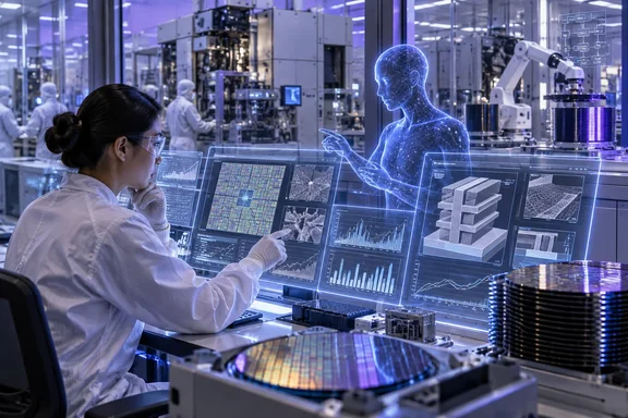
Speaking at National Taiwan University, Mii characterized AI as a “three-year-old Superman” — powerful but unable to reliably judge consequences. The Taipei Times, which independently reported the September 15 appearance, said Mii warned that AI remains weak when research moves into unknown territory, particularly where the underlying data does not yet exist. Wccftech’s account adds that he framed the problem around next-generation manufacturing: if current equipment and materials cannot meet a target, an AI model cannot reason its way past the physical limitation.
That distinction is more consequential than it sounds. The semiconductor industry is already applying machine learning in places where historical data is abundant and outcomes can be measured: finding bugs in RTL code, tuning chip floorplans, optimizing power and timing, and improving the enormous number of parameters involved in electronic design automation. But a new process node is not merely a bigger optimization job. It requires new transistor structures, interconnect methods, materials, masks, deposition steps, lithography processes, metrology and yield-control techniques that have to work together on actual wafers.
AI Can Optimize a Known System, Not Invent a Working Fab Process
Mii’s position is not a rejection of AI in chipmaking. TSMC is already using AI tools, and he specifically described coding and chip-design work as areas where the technology can deliver value. Those are comparatively structured domains: engineers can set constraints, simulate results, validate changes and feed the outcome back into the process.
Leading-edge process development has a different failure mode. A design tool can search a bounded space of viable options when it knows the rules of the system. A foundry R&D team working beyond an established node often has to discover the rules first. The data set may be incomplete, confidential, inconsistent across experiments, or simply nonexistent because no one has produced the relevant structures at scale.
That is the practical meaning behind Mii’s warning about “unknown” territory. AI can propose a process adjustment based on earlier runs, but it cannot prove that a new material will be stable through thousands of production cycles, that a novel transistor geometry can be patterned within tolerance, or that a process will deliver acceptable yields after it is transferred from an R&D line to a high-volume fab. Those questions are settled by experiments, measurement and engineering judgment, not fluent output from a model.
The industry may still see AI shorten parts of that loop. Better models can help identify promising experiments, correlate defects with tool settings, predict wafer variation and allocate engineers’ attention. But TSMC’s operations chief is describing AI as an accelerator inside a human-led research process, rather than an autonomous replacement for process engineers.
A14 Is a Manufacturing Program, Not a Single “1.4nm” Feature
The timing of Mii’s comments matters because TSMC is progressing from its 2nm generation toward A14, the platform generally described as 1.4nm-class. The naming should be read as a process-generation label, not as a literal measurement of a transistor gate or another individual feature. Modern node names no longer map cleanly to one physical dimension, and comparisons across chipmakers require more than a nanometer label.
TSMC’s own 2026 technology disclosures describe A14 as its second-generation nanosheet-transistor platform. At its July earnings call, the company said that A14 development was on track, with risk production planned for 2027 and volume manufacturing scheduled for 2028. TSMC also said internal test vehicles had reached close to 90 percent of targeted device performance and close to 90 percent yield for a 256-megabit SRAM test structure.
Those details put an important limit on the broad claim that AI cannot overcome manufacturing constraints. TSMC is not saying A14 is stalled or that the company lacks a route to production. Its public roadmap says the opposite: A14 is advancing toward its planned 2028 volume ramp. Mii’s point is that the progress will continue to depend on the work of specialists dealing with unresolved physical and production problems, even if AI becomes deeply embedded in their tools.
TSMC has also expanded the planned A14 family. The company announced A13 as an optical-shrink derivative intended to reduce die area while remaining compatible with A14 design rules, and A12 as a later A14-platform enhancement that adds the company’s Super Power Rail backside-power-delivery technology. TSMC currently schedules both A13 and A12 for production in 2029.
For the PC market, this means the more relevant question is not whether an AI agent can “design 1.4nm.” It is whether future desktop, notebook and data-center chips can afford the cost, design complexity and packaging demands of these nodes. The answer will depend on yields, wafer prices, power-delivery design, advanced packaging capacity and each chip designer’s ability to turn process advantages into a product worth paying for.
The Bottleneck Is Moving From Logic Design to Factory Reality
AI has already altered the economics of chip design. Modern processors contain billions of transistors, and the rules governing placement, routing, timing closure, verification and power management are too complex for wholly manual workflows. Cadence and Synopsys have both built AI-assisted capabilities into their design platforms, while chip designers increasingly use machine learning to explore a huge number of implementation choices.
This can make a large difference to the final product. A better physical layout may improve clock speed, cut power use or permit a smaller die. Faster verification may reduce the time required to reach tape-out. In a market where a few months can affect a CPU, GPU or AI accelerator launch, those gains have obvious commercial value.
Yet tape-out is only the handoff from a customer’s design team to the foundry. Manufacturing a working, economical chip at a new node is a separate challenge. The foundry must consistently print extremely small patterns, control defects, form transistors with predictable characteristics and connect billions of devices across many layers of metal. It then has to repeat that process at yields high enough to support real products.
A model trained on past process data can be very good at detecting relationships humans overlook. It cannot turn an unavailable material, unproven tool capability or unresolved lithography limit into a mature production step. Mii’s formulation is blunt, but it describes the division of labor accurately: automation improves a known operation; frontier R&D must establish a new one.
That is also why TSMC’s competitive edge cannot be reduced to node announcements. The company’s value to AMD, Apple, Nvidia, Qualcomm and other customers rests on taking difficult technology from a roadmap slide through risk production and into a reliable manufacturing ramp. A process that has attractive theoretical density or power characteristics but poor yields is not a viable platform for high-volume PC silicon.
Confidential Data Limits the AI Rollout Inside TSMC
Mii also highlighted another obstacle to treating AI as a universal engineering assistant: sensitive data. The Taipei Times reported that TSMC is cautious about using AI on confidential research and development information because of risks involving data leakage or corruption.
That concern applies sharply to advanced foundry development. Process recipes, defect data, yield-learning records, mask details and customer design information are among the most commercially sensitive assets in the technology industry. Feeding them into a third-party or inadequately controlled AI system is not a routine productivity decision. It is a security, intellectual-property and customer-trust decision.
The caution has relevance beyond TSMC. Enterprises rushing to deploy coding copilots and agentic tools often focus on prompt quality and productivity metrics first. Semiconductor work illustrates why data classification and access controls need to come before broad rollout. A model that can assist with source code or documentation may be acceptable in one environment and completely inappropriate for proprietary process development, unreleased chip layouts or production telemetry.
For IT administrators, the lesson is less glamorous than autonomous engineering but more actionable: AI governance needs to distinguish between work that can be safely processed in a controlled service and material that must remain inside a tightly governed environment. TSMC’s stance suggests that even a company positioned at the center of the AI hardware boom is not treating AI access as an all-or-nothing choice.
The Human Constraint Extends to TSMC’s Overseas Expansion
Mii also reportedly pointed to a less technical limitation in TSMC’s global buildout: recruiting senior managers capable of leading international teams. That is an unusually direct acknowledgment from a company expanding advanced manufacturing capacity across Taiwan, the United States, Japan and Europe.
New fabs require capital equipment, engineers, technicians, suppliers and reliable utilities, but leadership capacity is a constraint that cannot be fixed by ordering more tools. A company can replicate a fab design more easily than it can reproduce decades of operational knowledge about yield learning, manufacturing discipline, customer coordination and workforce management.
TSMC’s A14 roadmap remains pointed at a 2028 volume-production target, while its A12 and A13 extensions are targeted for 2029. Those dates are not promises of consumer products; chip customers still have to design parts, secure capacity and bring complete systems to market. But they show that the company’s development pipeline is advancing even as its operations chief cautions against imagining AI as a shortcut around the hardest work.
For Windows PC users, that leaves a straightforward conclusion: AI may help create the next generation of processors faster and with better efficiency, but it will not erase the slow, expensive, human-led work that determines whether those chips reach laptops, desktops and servers in volume.
References
- TSMC’s Operations Boss Says AI Cannot Fully Overcome Limitations To Design Next-Generation Chip Manufacturing Tech Such as 1.4-nanometer Node Wccftech · 2026-09-19T13:26:30+00:00