

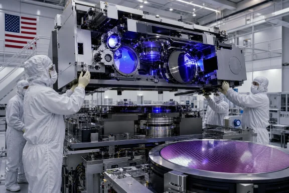
The first major modules of ASML’s High-NA extreme ultraviolet lithography system have begun arriving at NY Creates’ Albany NanoTech Complex, turning one of America’s most ambitious semiconductor research projects from a construction program into an operational technology platform. The July 21 delivery of the system’s bottom main module is more than a logistical milestone: it starts the painstaking assembly of a machine intended to help researchers develop chip processes beyond today’s leading nodes, while giving qualified U.S. companies and research partners access to capabilities that were previously concentrated within a small number of global chipmakers and overseas institutes.
New York Governor Kathy Hochul announced that NY Creates had received the first substantial components of ASML’s High-NA EUV system at the Albany NanoTech Complex. More modules are scheduled to arrive through the summer of 2026, followed by installation, integration, calibration and a lengthy process-development phase.
The equipment will anchor the new High-NA EUV Lithography Center inside the NanoFab Reflection building. New York State has committed $1 billion to the expansion, which officials say is leveraging approximately $9 billion in industry investment from partners across the semiconductor ecosystem.
The arrival follows the April 2026 delivery of a Tokyo Electron CLEAN TRACK LITHIUS Pro DICE coater and developer. That system prepares wafers with light-sensitive photoresist, processes them around the exposure stage and forms an essential part of the lithography workflow.
The sequence is likely to include:
Researchers in Albany subsequently produced full-field EUV test chips, helping the industry understand how the difficult technology might move from experimental tools to practical fabrication. EUV eventually became central to manufacturing advanced processors used in premium PCs, smartphones, servers, graphics accelerators and AI hardware.
The High-NA installation therefore represents a continuation of Albany’s lithography work rather than a wholly new direction. The difference is the scale of the new center and the strategic importance now attached to domestic semiconductor capacity.
Its value comes from the concentration of cleanrooms, wafer-processing equipment and technical expertise. Semiconductor research cannot be performed effectively with a lithography scanner in isolation; wafers must pass through deposition, etching, cleaning, inspection, metrology and packaging-related processes before useful conclusions can be drawn.
Albany’s advantage is the surrounding process ecosystem. The High-NA scanner adds a critical capability to an environment already built around 300-millimeter wafer research and collaboration with major industry partners.
Generating usable EUV light is exceptionally difficult. A high-powered laser strikes tiny droplets of molten tin, creating plasma that emits EUV radiation. The light must then be collected, shaped and directed through a vacuum environment.
Ordinary lenses cannot perform the task because most materials absorb EUV light. The system instead uses exceptionally smooth multilayer mirrors to reflect and focus the radiation through the optical path.
Higher numerical aperture improves resolution without requiring a shorter wavelength. ASML says its first-generation EXE:5000 can provide 8-nanometer resolution and print features roughly 1.7 times smaller than those enabled by the preceding 0.33-NA EUV platform under comparable assumptions.
The increase is technically demanding because the system must handle light traveling through the projection optics at larger angles. ASML and optics partner Zeiss developed larger, anamorphic mirrors that apply different reduction factors across the two directions of the image.
That introduces new challenges for chip designers and fabrication engineers. Large dies may require stitching strategies or modified layouts, while the scanner needs faster reticle and wafer stages to preserve economically useful throughput.
High-NA EUV therefore improves resolution but does not make process development simpler in every respect. It exchanges some forms of multiple-patterning complexity for new optical, mask, layout and stitching considerations.
A simplified comparison illustrates the trade-off:
Those gains matter because a tiny variation can become a defective transistor, broken connection or electrical characteristic outside the intended range. On a wafer containing billions or trillions of patterned features, small statistical improvements can translate into significant yield and performance benefits.
However, scanner specifications do not automatically become production yields. Researchers must optimize the complete stack of photoresist, mask, exposure dose, wafer processing and measurement.
Modern chips contain many relevant measurements, including gate pitch, metal pitch, contact dimensions and interconnect spacing. Different manufacturers can also use the same nominal node label for processes with different density, power and performance characteristics.
A “sub-1-nanometer” research program therefore refers to future process generations beyond the currently emerging angstrom-class era. It does not mean that Albany will immediately print complete commercial transistors measuring less than one nanometer in every direction.
High-NA EUV could assist with critical layers in those architectures, but it cannot solve every scaling barrier. Heat, resistance, capacitance, quantum effects, material limits and manufacturing variability become increasingly important as devices grow denser.
The scanner enables experiments that would otherwise be impossible or impractical; it does not guarantee that every experiment will become a commercially viable process.
That distinction could matter to:
This creates the potential for Albany to serve two related missions. It can support the New York-backed public-private research partnership while also providing infrastructure for broader national semiconductor programs.
The long-term test will be whether the center can translate shared equipment into faster commercialization. Access alone has limited value if researchers face excessive queues, inflexible agreements or barriers to moving successful processes into production facilities.
The building is not simply an enclosure. Minute temperature changes, floor movement or airborne contamination can interfere with advanced semiconductor processing, so the surrounding facility becomes part of the tool’s effective performance envelope.
State officials say the investment is leveraging $9 billion from industry participants, creating a $10 billion initiative. Partners associated with the broader project have included IBM, Micron, Applied Materials, Tokyo Electron and other major semiconductor companies.
Precompetitive research allows multiple participants to investigate common technical barriers before differentiating their commercial products. Shared facilities can reduce duplicated capital expenditure while giving equipment suppliers feedback from a broader set of users.
The arrangement must nevertheless protect sensitive information. Contracts, physical separation, data controls and carefully defined research scopes will determine whether competing organizations trust the platform.
That distinction matters because semiconductor leadership is not secured by constructing a single factory. The industry advances continuously, and a facility that is competitive at opening can fall behind if it lacks access to the next manufacturing technology.
High-NA research in the United States could help shorten the distance between laboratory work and domestic production. It could also provide a neutral environment where process modules are tested before being transferred to commercial fabs.
The Albany project should therefore be understood as a resilience measure rather than a claim of technological self-sufficiency. The United States gains domestic access, expertise and process-development capacity while remaining connected to allied suppliers.
That model may be more practical than attempting to recreate every specialized component within national borders. Modern semiconductor manufacturing is deeply international, and resilience can come from diversified, trusted networks rather than complete isolation.
Albany’s opportunity lies in creating a comparable center of gravity for North American research. Its existing equipment base, history with EUV and connection to federal programs offer a foundation, but reputation will depend on technical results and partner experience rather than announcements.
The competition is also complementary. Semiconductor companies often participate in multiple research ecosystems, and discoveries made at one institute can drive equipment or materials development that benefits the industry more broadly.
IBM has a long history of semiconductor research in New York and has used Albany partnerships to demonstrate new transistor technologies. The High-NA center could extend that model into future nodes, even though IBM no longer operates a large leading-edge merchant foundry.
Micron’s planned memory investments in Central New York add another regional dimension. High-NA EUV is expected eventually to influence advanced memory manufacturing, although the timing and economics will differ from leading-edge logic.
For Windows laptops, efficiency may matter more than raw peak speed. Reduced power consumption can improve battery life, support thinner designs and lower cooling requirements, although system-level results still depend on architecture, software and manufacturing choices.
More advanced process nodes could make room for larger NPUs or more specialized accelerators. They might also support improved packaging configurations that place compute, cache and memory closer together.
High-NA lithography will not determine whether AI features are useful, private or well designed. It can, however, expand the hardware envelope within which Windows developers and device makers operate.
High-NA systems, masks and supporting processes carry enormous costs. Fewer patterning steps may reduce per-layer complexity, yet the scanner itself must achieve sufficient utilization and throughput for those savings to offset capital and operating expenses.
Consumers should not assume that smaller nodes automatically mean cheaper PCs. Chip prices also reflect design cost, packaging, memory, product positioning, competition and the number of usable dies produced from each wafer.
High-NA EUV could help fabricate denser compute tiles and selected interconnect structures. The resulting systems may support larger workloads within the same data-center power budget, although escalating model demand could consume those efficiency gains.
Enterprise customers are unlikely to choose hardware based on whether High-NA EUV was used. They will evaluate total cost of ownership, software compatibility, security, power consumption and workload performance.
The technology’s impact will therefore appear indirectly through better products, not as a customer-facing feature. No Windows administrator will enable “High-NA mode,” but administrators may manage systems whose capabilities depended on High-NA processes several years earlier.
Potential workforce needs include:
Recruitment alone will not solve the problem. New York will need to retain workers through competitive compensation, career development, housing availability and stable long-term research programs.
After first light, attention will shift toward imaging performance. Researchers will need to establish overlay accuracy, focus control, defect rates, dose behavior and compatibility with the surrounding process tools.
Masks present their own issues, including three-dimensional effects, inspection requirements and the anamorphic imaging system. Progress in these supporting technologies will determine how quickly the scanner becomes a productive research instrument.
Important questions include:
That evidence may take years to emerge. Early indicators could include new materials qualified for High-NA, supplier products developed with Albany data, transistor demonstrations and formal process-transfer agreements with domestic fabs.
If the center works as intended, it could help U.S. researchers solve process problems before they reach factories, broaden access to tools normally reserved for the largest chipmakers and train a workforce capable of supporting future fabrication. That could eventually influence everything from Windows laptops and AI PCs to cloud servers, automotive systems and national-security hardware.
The difficult phase now begins. ASML’s modules must become a stable scanner, the scanner must become a productive research platform, and that platform must generate processes industry can manufacture economically. Albany has secured the equipment needed to compete at the frontier; the next test is whether it can turn that extraordinary hardware into repeatable innovation.
 Overview
New York Governor Kathy Hochul announced that NY Creates had received the first substantial components of ASML’s High-NA EUV system at the Albany NanoTech Complex. More modules are scheduled to arrive through the summer of 2026, followed by installation, integration, calibration and a lengthy process-development phase.The equipment will anchor the new High-NA EUV Lithography Center inside the NanoFab Reflection building. New York State has committed $1 billion to the expansion, which officials say is leveraging approximately $9 billion in industry investment from partners across the semiconductor ecosystem.
What arrived in Albany
The latest delivery includes the bottom main module, a foundational part of an ASML High-NA EUV scanner. These systems are not shipped as complete machines; their size, complexity and sensitivity require transportation in multiple specially protected modules that are assembled inside the destination cleanroom.The arrival follows the April 2026 delivery of a Tokyo Electron CLEAN TRACK LITHIUS Pro DICE coater and developer. That system prepares wafers with light-sensitive photoresist, processes them around the exposure stage and forms an essential part of the lithography workflow.
The immediate timeline
NY Creates previously said that “first light,” the point at which the assembled scanner initially generates EUV light, was expected before the end of 2026. First light would be a major achievement, but it would not mean that the machine was ready for advanced production research on the following day.The sequence is likely to include:
- Specialized crews will move and position each module inside the cleanroom while maintaining strict vibration, contamination and environmental controls.
- Engineers will mechanically and electrically integrate the system, including its light source, vacuum environment, optics, stages and supporting infrastructure.
- ASML and site personnel will calibrate the scanner to extraordinary levels of positional and optical precision.
- Researchers will qualify materials, masks, resists and process conditions using the Tokyo Electron track and other supporting tools.
- The center will develop repeatable process modules that outside partners can use for experiments and future manufacturing research.
Albany’s Long Semiconductor History
Albany did not emerge suddenly as a semiconductor research location. The region has spent more than two decades building a shared research model in which government, universities, equipment companies and chip designers can collaborate around expensive infrastructure.From early EUV experiments to High-NA
Albany was involved in EUV development long before the technology entered mainstream chip production. In 2006, ASML shipped an early EUV demonstration system to what was then the College of Nanoscale Science and Engineering in Albany, while another went to the Belgian research institute imec.Researchers in Albany subsequently produced full-field EUV test chips, helping the industry understand how the difficult technology might move from experimental tools to practical fabrication. EUV eventually became central to manufacturing advanced processors used in premium PCs, smartphones, servers, graphics accelerators and AI hardware.
The High-NA installation therefore represents a continuation of Albany’s lithography work rather than a wholly new direction. The difference is the scale of the new center and the strategic importance now attached to domestic semiconductor capacity.
A substantial existing research campus
The Albany NanoTech Complex encompasses approximately 1.65 million square feet and has attracted more than $25 billion in cumulative high-technology investment. Roughly 3,000 research and development jobs are located at the site, according to NY Creates.Its value comes from the concentration of cleanrooms, wafer-processing equipment and technical expertise. Semiconductor research cannot be performed effectively with a lithography scanner in isolation; wafers must pass through deposition, etching, cleaning, inspection, metrology and packaging-related processes before useful conclusions can be drawn.
Albany’s advantage is the surrounding process ecosystem. The High-NA scanner adds a critical capability to an environment already built around 300-millimeter wafer research and collaboration with major industry partners.
How High-NA EUV Works
Lithography transfers circuit patterns from a photomask, also called a reticle, onto a light-sensitive layer deposited on a silicon wafer. The smaller and more accurately those patterns can be printed, the more flexibility chipmakers gain when designing dense, efficient devices.Why EUV uses such unusual light
Current EUV systems use light with a wavelength of approximately 13.5 nanometers. This is far shorter than the 193-nanometer wavelength used by deep ultraviolet immersion lithography systems, allowing EUV tools to resolve considerably smaller features.Generating usable EUV light is exceptionally difficult. A high-powered laser strikes tiny droplets of molten tin, creating plasma that emits EUV radiation. The light must then be collected, shaped and directed through a vacuum environment.
Ordinary lenses cannot perform the task because most materials absorb EUV light. The system instead uses exceptionally smooth multilayer mirrors to reflect and focus the radiation through the optical path.
What numerical aperture changes
Numerical aperture describes an optical system’s ability to collect and focus light. ASML’s established NXE EUV platform uses a numerical aperture of 0.33, while the EXE High-NA platform raises that figure to 0.55.Higher numerical aperture improves resolution without requiring a shorter wavelength. ASML says its first-generation EXE:5000 can provide 8-nanometer resolution and print features roughly 1.7 times smaller than those enabled by the preceding 0.33-NA EUV platform under comparable assumptions.
The increase is technically demanding because the system must handle light traveling through the projection optics at larger angles. ASML and optics partner Zeiss developed larger, anamorphic mirrors that apply different reduction factors across the two directions of the image.
A smaller exposure field
The anamorphic design allows existing reticle dimensions to remain usable, avoiding an industry-wide transition to larger masks. However, High-NA EUV exposes a field that is half the size of the conventional EUV field.That introduces new challenges for chip designers and fabrication engineers. Large dies may require stitching strategies or modified layouts, while the scanner needs faster reticle and wafer stages to preserve economically useful throughput.
High-NA EUV therefore improves resolution but does not make process development simpler in every respect. It exchanges some forms of multiple-patterning complexity for new optical, mask, layout and stitching considerations.
Why the Equipment Matters
High-NA EUV is expected to support multiple generations of leading-edge logic and memory development. Its primary promise is the ability to print selected critical layers with fewer patterning steps than would otherwise be required.Reducing multiple patterning
When a lithography tool cannot print a sufficiently dense pattern in one exposure, manufacturers can divide that pattern across two or more masks and processing cycles. This technique extends the life of an existing lithography platform, but every additional cycle adds cost, time and opportunities for error.A simplified comparison illustrates the trade-off:
- Single-pattern High-NA exposure can reduce the number of masks and process steps required for certain dense layers.
- Multiple-pattern conventional EUV can remain preferable when its mature infrastructure and throughput produce better economics.
- Deep ultraviolet lithography will continue serving many less critical layers, because using an EUV scanner everywhere would be unnecessary and prohibitively expensive.
- The final process will mix several lithography technologies, depending on resolution, yield, cost and reliability requirements.
Improving pattern fidelity
ASML reports that the EXE:5000 offers substantially higher imaging contrast than its NXE systems. Better contrast can produce a clearer distinction between exposed and unexposed resist, potentially improving the consistency of fine patterns.Those gains matter because a tiny variation can become a defective transistor, broken connection or electrical characteristic outside the intended range. On a wafer containing billions or trillions of patterned features, small statistical improvements can translate into significant yield and performance benefits.
However, scanner specifications do not automatically become production yields. Researchers must optimize the complete stack of photoresist, mask, exposure dose, wafer processing and measurement.
The Meaning of “Sub-1 Nanometer” Development
New York’s announcement says the center will help drive sub-1-nanometer chip development. That description signals the intended longevity of the facility, but it should not be interpreted as a literal measurement of every transistor feature.Node names are no longer physical dimensions
Names such as 7 nm, 5 nm, 3 nm and 2 nm have evolved into generational labels. They identify a broad process family and its expected improvements rather than a single transistor dimension that precisely matches the advertised number.Modern chips contain many relevant measurements, including gate pitch, metal pitch, contact dimensions and interconnect spacing. Different manufacturers can also use the same nominal node label for processes with different density, power and performance characteristics.
A “sub-1-nanometer” research program therefore refers to future process generations beyond the currently emerging angstrom-class era. It does not mean that Albany will immediately print complete commercial transistors measuring less than one nanometer in every direction.
Lithography is only part of scaling
Future chips will depend on more than shrinking conventional planar dimensions. Researchers are exploring gate-all-around transistors, complementary field-effect transistor structures, backside power delivery, new interconnect materials and increasingly sophisticated three-dimensional integration.High-NA EUV could assist with critical layers in those architectures, but it cannot solve every scaling barrier. Heat, resistance, capacitance, quantum effects, material limits and manufacturing variability become increasingly important as devices grow denser.
The scanner enables experiments that would otherwise be impossible or impractical; it does not guarantee that every experiment will become a commercially viable process.
An Accessible National Research Asset
High-NA EUV machines are extraordinarily expensive and scarce. The first systems have naturally gone to the world’s largest semiconductor manufacturers and research organizations, which can support the equipment and justify its cost.Opening access beyond the largest chipmakers
Albany’s defining proposition is shared access. NY Creates describes the project as North America’s first accessible High-NA EUV Lithography Center and the first publicly owned center of its type in the region.That distinction could matter to:
- Semiconductor manufacturers that need precompetitive process research before committing capacity inside production fabs.
- Equipment and materials suppliers that must test products under realistic High-NA conditions.
- Universities and government-backed programs that could not independently acquire such equipment.
- Smaller chip companies that need research pathways but lack their own leading-edge fabrication facilities.
- Workforce programs that require practical exposure to advanced manufacturing systems.
The role of the NSTC
The Albany NanoTech Complex was selected as the planned location of the CHIPS for America Extreme Ultraviolet Accelerator, a flagship research facility associated with the National Semiconductor Technology Center. The federal plan announced in 2024 contemplated an investment of approximately $825 million and access to both conventional and High-NA EUV capabilities.This creates the potential for Albany to serve two related missions. It can support the New York-backed public-private research partnership while also providing infrastructure for broader national semiconductor programs.
The long-term test will be whether the center can translate shared equipment into faster commercialization. Access alone has limited value if researchers face excessive queues, inflexible agreements or barriers to moving successful processes into production facilities.
The Public-Private Investment Model
The project combines state funding, private commitments and federal semiconductor policy. That structure reflects the reality that leading-edge semiconductor research has become too expensive for most individual organizations to pursue alone.New York’s billion-dollar commitment
New York’s $1 billion contribution supports NanoFab Reflection and the infrastructure required for advanced lithography research. The facility must provide cleanroom conditions, stable power, chilled water, vacuum systems, contamination control and vibration management suitable for one of the most precise machines ever built.The building is not simply an enclosure. Minute temperature changes, floor movement or airborne contamination can interfere with advanced semiconductor processing, so the surrounding facility becomes part of the tool’s effective performance envelope.
State officials say the investment is leveraging $9 billion from industry participants, creating a $10 billion initiative. Partners associated with the broader project have included IBM, Micron, Applied Materials, Tokyo Electron and other major semiconductor companies.
Why companies cooperate with competitors
Semiconductor companies compete aggressively in products and manufacturing, but they also share foundational problems. No single chipmaker controls every part of the supply chain, which spans lithography, materials, optics, deposition, etching, inspection, design software and packaging.Precompetitive research allows multiple participants to investigate common technical barriers before differentiating their commercial products. Shared facilities can reduce duplicated capital expenditure while giving equipment suppliers feedback from a broader set of users.
The arrangement must nevertheless protect sensitive information. Contracts, physical separation, data controls and carefully defined research scopes will determine whether competing organizations trust the platform.
Implications for the U.S. Chip Strategy
The United States remains a leader in semiconductor design, equipment and software, but much of the world’s most advanced chip manufacturing capacity has been concentrated in East Asia. Recent industrial policy has sought to expand domestic fabrication while reinforcing research, workforce and supply-chain capabilities.R&D must accompany new fabs
Building fabrication plants without a supporting research ecosystem can produce domestic capacity that depends heavily on processes developed elsewhere. Albany addresses a different part of the problem by concentrating on the methods and tools needed for future generations.That distinction matters because semiconductor leadership is not secured by constructing a single factory. The industry advances continuously, and a facility that is competitive at opening can fall behind if it lacks access to the next manufacturing technology.
High-NA research in the United States could help shorten the distance between laboratory work and domestic production. It could also provide a neutral environment where process modules are tested before being transferred to commercial fabs.
Supply-chain resilience has limits
Installing an ASML scanner in New York does not create a fully domestic semiconductor supply chain. ASML is headquartered in the Netherlands, its critical optics come from Germany, and the broader system relies on a specialized global supplier network.The Albany project should therefore be understood as a resilience measure rather than a claim of technological self-sufficiency. The United States gains domestic access, expertise and process-development capacity while remaining connected to allied suppliers.
That model may be more practical than attempting to recreate every specialized component within national borders. Modern semiconductor manufacturing is deeply international, and resilience can come from diversified, trusted networks rather than complete isolation.
Competitive Implications
Albany will operate in a global research landscape that includes imec in Belgium and advanced development programs within Intel, TSMC, Samsung and major memory manufacturers. Those organizations are also learning how High-NA EUV behaves in realistic process environments.Competition with established research hubs
Imec has built a powerful position as a neutral semiconductor research institute with close links to chipmakers, equipment suppliers and universities. Its early access to High-NA EUV gives it an important head start in materials, imaging and process integration.Albany’s opportunity lies in creating a comparable center of gravity for North American research. Its existing equipment base, history with EUV and connection to federal programs offer a foundation, but reputation will depend on technical results and partner experience rather than announcements.
The competition is also complementary. Semiconductor companies often participate in multiple research ecosystems, and discoveries made at one institute can drive equipment or materials development that benefits the industry more broadly.
Potential benefits for Intel and IBM
Intel has committed heavily to High-NA EUV and received the first commercial EXE:5000 system from ASML in late 2023. Albany may provide an additional venue for ecosystem development, supplier qualification and research that supports future U.S. manufacturing.IBM has a long history of semiconductor research in New York and has used Albany partnerships to demonstrate new transistor technologies. The High-NA center could extend that model into future nodes, even though IBM no longer operates a large leading-edge merchant foundry.
Micron’s planned memory investments in Central New York add another regional dimension. High-NA EUV is expected eventually to influence advanced memory manufacturing, although the timing and economics will differ from leading-edge logic.
What This Could Mean for Windows PCs
The Albany installation will not cause an immediate change in Windows hardware. Process research typically takes years to mature into qualified manufacturing, followed by product design, validation and commercial release.Faster and more efficient processors
If High-NA EUV helps manufacturers build denser transistors with acceptable yields, future PC processors could deliver more performance within a given power envelope. Designers might use the additional transistor budget for CPU cores, graphics, cache, media engines, security functions or neural processing units.For Windows laptops, efficiency may matter more than raw peak speed. Reduced power consumption can improve battery life, support thinner designs and lower cooling requirements, although system-level results still depend on architecture, software and manufacturing choices.
More capable local AI
Microsoft and PC manufacturers have been promoting AI PCs equipped with dedicated NPUs. Running larger models locally requires substantial compute capability, memory bandwidth and efficient data movement, all of which increase pressure on silicon area and power.More advanced process nodes could make room for larger NPUs or more specialized accelerators. They might also support improved packaging configurations that place compute, cache and memory closer together.
High-NA lithography will not determine whether AI features are useful, private or well designed. It can, however, expand the hardware envelope within which Windows developers and device makers operate.
Affordability is not guaranteed
New York’s announcement links next-generation research to faster, more efficient and more affordable chips. The first two outcomes are plausible technical goals, but affordability is complicated.High-NA systems, masks and supporting processes carry enormous costs. Fewer patterning steps may reduce per-layer complexity, yet the scanner itself must achieve sufficient utilization and throughput for those savings to offset capital and operating expenses.
Consumers should not assume that smaller nodes automatically mean cheaper PCs. Chip prices also reflect design cost, packaging, memory, product positioning, competition and the number of usable dies produced from each wafer.
Enterprise and Data-Center Impact
Enterprise computing may see some of the earliest benefits from future leading-edge processes because servers and AI accelerators can justify premium manufacturing costs. Data centers place a high economic value on performance per watt, density and reliability.AI infrastructure
Advanced AI processors combine vast amounts of compute with high-bandwidth memory and complex packaging. Lithographic scaling can improve logic density, but the industry must also solve power delivery, heat removal and communication bottlenecks.High-NA EUV could help fabricate denser compute tiles and selected interconnect structures. The resulting systems may support larger workloads within the same data-center power budget, although escalating model demand could consume those efficiency gains.
Windows Server and cloud services
Future server CPUs manufactured with High-NA-enabled processes could provide more cores, larger caches and stronger acceleration for encryption, virtualization and AI inference. Those improvements would eventually influence Windows Server deployments and Microsoft’s cloud infrastructure.Enterprise customers are unlikely to choose hardware based on whether High-NA EUV was used. They will evaluate total cost of ownership, software compatibility, security, power consumption and workload performance.
The technology’s impact will therefore appear indirectly through better products, not as a customer-facing feature. No Windows administrator will enable “High-NA mode,” but administrators may manage systems whose capabilities depended on High-NA processes several years earlier.
Workforce and Regional Effects
The project is expected to create hundreds of permanent jobs, in addition to construction and installation work. The broader economic impact could extend to suppliers, universities and technical training programs across New York.Jobs beyond advanced physics
A High-NA center needs optical and process experts, but it also depends on technicians, facilities engineers, electricians, software specialists, safety personnel and equipment-maintenance teams. Semiconductor operations require disciplined execution across a wide range of occupations.Potential workforce needs include:
- Process engineers who develop and stabilize lithography recipes.
- Equipment technicians who maintain complex vacuum, optical and mechanical systems.
- Metrology specialists who measure structures and diagnose defects.
- Materials scientists who develop resists, films and cleaning chemistries.
- Automation and software engineers who manage data, scheduling and tool control.
- Facilities personnel who maintain uninterrupted cleanroom utilities.
Competition for specialized talent
Albany must compete with semiconductor clusters in Arizona, Texas, Oregon, California and overseas markets. The expansion of U.S. chip investment is increasing demand for many of the same scarce skills.Recruitment alone will not solve the problem. New York will need to retain workers through competitive compensation, career development, housing availability and stable long-term research programs.
Strengths and Opportunities
The Albany High-NA EUV center combines rare equipment with an established research environment. Its strongest opportunities extend beyond the prestige of owning an advanced scanner.- Shared access can reduce barriers to experimentation. Companies and researchers may test materials and process concepts without purchasing their own High-NA system.
- Albany already has a substantial semiconductor ecosystem. Existing cleanrooms, tools, partners and expertise should make integration more practical than building an isolated center from scratch.
- The project can connect research with domestic manufacturing. Successful processes may eventually transfer to U.S. logic, memory and specialty-chip facilities.
- Supplier innovation could accelerate. Resist developers, mask companies, metrology vendors and process-equipment makers need realistic High-NA environments to refine their products.
- Workforce development can become hands-on. Training around operational advanced tools is more valuable than classroom instruction disconnected from fabrication conditions.
- The center may strengthen allied technology networks. Albany brings Dutch lithography systems, German optics, Japanese wafer-processing equipment and American research capabilities into one platform.
- Public ownership can support long-term research. A shared institution may pursue foundational work that commercial fabs would postpone in favor of immediate production priorities.
Risks and Concerns
The project’s promise should be balanced against substantial execution, economic and policy risks. High-NA EUV remains a developing production technology, and a successful installation does not automatically produce commercially useful research.- Integration could take longer than expected. Complex modules must work together at extreme precision, and first light is only one stage in a lengthy qualification process.
- Tool utilization may become a bottleneck. Demand from multiple partners could exceed available scanner time, limiting practical accessibility.
- Operating costs will be high. Maintenance, consumables, utilities, masks, resists and specialized staff will require sustained funding after the construction phase.
- High-NA economics remain process-dependent. Some layers may continue using conventional EUV multiple patterning if it offers better cost or throughput.
- Half-field imaging introduces design complications. Large dies may need stitching or layout changes that offset some benefits.
- Research access can conflict with intellectual-property protection. Partners must trust that sensitive process data and experimental results remain secure.
- Political priorities can change. Semiconductor programs require support over decades, while public budgets and administrations operate on much shorter cycles.
- Regional investment does not guarantee domestic mass production. Processes developed in Albany could ultimately be adopted by fabs outside the United States unless transfer and commercialization pathways remain competitive.
- The project depends on an international supply chain. Export controls, trade disputes or supplier disruptions could affect parts, upgrades and service.
What to Watch Next
The next several months will reveal whether construction and tool installation remain on schedule. The most visible milestone will be first light, but more meaningful evidence will come from wafer exposures, process qualifications and partner research programs.Installation and calibration
Observers should watch for confirmation that all principal ASML modules have arrived and that mechanical integration is complete. The facility must also demonstrate that its environmental infrastructure meets the scanner’s requirements.After first light, attention will shift toward imaging performance. Researchers will need to establish overlay accuracy, focus control, defect rates, dose behavior and compatibility with the surrounding process tools.
Resist and mask progress
High-NA EUV places demanding requirements on photoresists. A useful resist must resolve tiny features while maintaining sensitivity and limiting random defects, properties that can work against one another.Masks present their own issues, including three-dimensional effects, inspection requirements and the anamorphic imaging system. Progress in these supporting technologies will determine how quickly the scanner becomes a productive research instrument.
Access rules and project selection
NY Creates and its partners will need transparent mechanisms for allocating tool time. The strongest model would balance anchor-company research with opportunities for universities, suppliers and smaller participants.Important questions include:
- How will organizations apply for access?
- What costs will users bear?
- How will intellectual property be divided?
- Which experiments will receive priority?
- How quickly can successful work transfer into commercial manufacturing?
- What performance and economic results will be publicly reported?
Evidence of commercial transfer
The ultimate benchmark will not be the number of wafers exposed in Albany. It will be whether research performed there reduces the time, cost or risk of manufacturing future chips.That evidence may take years to emerge. Early indicators could include new materials qualified for High-NA, supplier products developed with Albany data, transistor demonstrations and formal process-transfer agreements with domestic fabs.
Looking Ahead
The arrival of ASML’s bottom main module gives New York a tangible foothold in the next era of semiconductor lithography, but the project’s importance extends beyond the machine. Albany is attempting to build an accessible research system around one of the industry’s rarest technologies, combining state infrastructure, federal strategy, private investment and international equipment expertise.If the center works as intended, it could help U.S. researchers solve process problems before they reach factories, broaden access to tools normally reserved for the largest chipmakers and train a workforce capable of supporting future fabrication. That could eventually influence everything from Windows laptops and AI PCs to cloud servers, automotive systems and national-security hardware.
The difficult phase now begins. ASML’s modules must become a stable scanner, the scanner must become a productive research platform, and that platform must generate processes industry can manufacture economically. Albany has secured the equipment needed to compete at the frontier; the next test is whether it can turn that extraordinary hardware into repeatable innovation.
References
- Primary source: Empire State Development (ESD) (.gov)
Published: 2026-07-21T17:07:51+00:00
- Related coverage: commerce.gov
Biden-Harris Administration Announces NY CREATES’ Albany NanoTech Complex as the first CHIPS for America R&D Flagship Facility and Planned Site for the estimated $825 Million CHIPS for America EUV Accelerator
October 31, 2024 – Washington, D.C. – Today, the Department of Commerce and Natcast, the operator of the National Semiconductor Technology Center (NSTC), announced the expected location for the first CHIPS for America research and development (R&D) flagship facility. www.commerce.gov
- Related coverage: ny-creates.org
