

Dr Farzan Gity of Tyndall National Institute has joined a highly selective global group after Intel named him one of 10 recipients of its 2025 Outstanding Researcher Awards. The recognition is more than an individual academic honor: it highlights research into one of the semiconductor industry’s most difficult long-term problems—how to preserve reliable electrical performance when transistor channels become so thin that individual defects can determine whether a device works as intended.
Intel’s annual Outstanding Researcher Awards recognize academics whose Intel-sponsored work combines fundamental insight, technical difficulty, effective collaboration, and potential industry relevance. The program is overseen by Intel’s Corporate Research Council and serves as one of the company’s mechanisms for connecting university research with future computing requirements.
Gity is a senior staff researcher at Tyndall National Institute, which is based at University College Cork in Ireland. He leads research into emerging materials and devices for nanoelectronics, information and communications technology, and spintronics, with a particular focus on technologies that could extend integrated-circuit development beyond the limits of conventional silicon scaling.
The breadth of the winning projects illustrates how semiconductor innovation has expanded beyond simply making transistors smaller. Future computing performance will depend on advances spanning materials science, packaging, chip architecture, software security, AI acceleration, thermal sensing, and manufacturing.
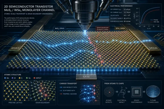
Gity received the award for a project titled “Role of Grain Boundaries in TMDs on Carrier Transport: Identifying GB Structure-Electrical Property Correlation.” The work examined how different grain-boundary configurations affect the movement of electrical carriers through two-dimensional transition metal dichalcogenide materials.
Gity serves as principal investigator for an Intel-funded project on two-dimensional materials and is also associated with Ireland’s AMBER research center. His team’s work combines material analysis, device fabrication, electrical characterization, and computational modelling—an interdisciplinary mixture that is increasingly necessary as chip development approaches atomic dimensions.
The award therefore recognizes not just a promising idea, but a research structure capable of connecting atomic-scale observations with consequences for functioning electronic devices.
Each grain can have a different orientation. Where two grains meet, the atomic pattern must adjust, creating a grain boundary.
That boundary is not simply a cosmetic imperfection. It can change local bonding, introduce electronic states, scatter carriers, create barriers to conduction, or produce paths with electrical behavior that differs from the surrounding material.
In an atomically thin transistor channel, there is little bulk material to average out those effects. A single boundary crossing the channel may influence resistance, current flow, variability, reliability, and the threshold at which the transistor switches.
That distinction is critical. Semiconductor manufacturing does not necessarily need every material to be atomically perfect, but engineers must understand which imperfections can be tolerated, which can be controlled, and which must be eliminated.
The research specifically considered molybdenum disulfide, or MoS₂, and tungsten diselenide, or WSe₂. Both belong to the TMD family and have attracted attention as possible channel materials for future transistors.
By combining modelling with experimental characterization, the project connected atomic-scale boundary structures to measurable device behavior. Those findings can help researchers refine material growth, select channel geometry, and design devices that remain functional even when large-area films contain unavoidable crystalline boundaries.
The problem becomes especially acute in monolayer materials. Their extreme thinness is one of their main advantages, but it also means electrical carriers cannot simply travel above, below, or around a disruptive region in the way they might within a thicker three-dimensional material.
Several possible effects can follow:
If nominally identical TMD transistors behave differently because a channel contains one boundary configuration rather than another, designers may need larger operating margins. Those margins can consume power, limit clock speeds, reduce manufacturing yield, or make the technology less competitive than alternatives.
This is why a map connecting boundary structure with electrical behavior is so valuable. It gives process engineers a way to move from the broad instruction “reduce defects” toward more actionable questions:
TMDs also provide semiconductor bandgaps, distinguishing them from graphene, whose lack of a natural bandgap complicates its use in conventional digital logic. MoS₂ and WSe₂ are among the most extensively studied TMDs because they offer complementary properties and can be investigated in transistor structures.
Their potential advantages include:
The atomic species, bonding arrangements, defect energetics, and electrical responses differ. Grain boundaries that severely restrict conduction in one material may produce a different outcome in another.
A comparative approach helps separate universal grain-boundary effects from material-specific behavior. It can also inform decisions about whether a particular TMD is suitable for a given transistor architecture or whether a combination of materials could provide better system-level performance.
The research does not mean that MoS₂ or WSe₂ is ready to replace silicon in mainstream processors. It instead addresses a prerequisite for any credible manufacturing roadmap: understanding how real, imperfect material behaves in real devices.
Modelling also helps explain why a measured device behaves in a particular way. If an experiment shows reduced current, the calculation can test whether a specific boundary structure would be expected to create the observed disruption.
However, simulations depend on assumptions. Material quality, contacts, substrates, dielectric layers, contamination, strain, and measurement conditions can all influence a physical device in ways that are difficult to reproduce perfectly in a model.
The most useful cycle is iterative:
A useful rule might connect a specific boundary orientation with a predictable resistance penalty, identify a structure that must be avoided, or show that a device architecture is relatively tolerant of certain defects. Such rules can feed into material-growth targets, transistor layout choices, compact device models, and statistical circuit analysis.
That transition—from atomic observation to manufacturable design guidance—is a major reason Intel-sponsored academic research can matter even when it sits years away from a shipping product.
Manufacturers are moving toward gate-all-around transistor structures, backside power delivery, chiplets, advanced interconnects, stacked dies, and increasingly complex packaging. Two-dimensional materials could eventually add another option, particularly where conventional channels encounter electrostatic or physical limits.
Their adoption would still require an extensive ecosystem. Equipment suppliers would need suitable deposition and inspection tools. Process engineers would need stable integration flows, while designers would need accurate models that work with electronic design automation software.
Research into grain boundaries belongs near the beginning of that chain. It provides information needed before manufacturers can establish acceptable defect densities, yield targets, and performance expectations.
If certain boundaries are highly disruptive while others are relatively benign, manufacturers may focus on suppressing the dangerous configurations rather than pursuing absolute perfection. That could produce a more realistic path toward scalable fabrication.
Device architects might also reduce sensitivity by changing channel dimensions, orientation, contact placement, or stacking arrangements. Circuit designers could incorporate statistical variation into libraries and timing models, provided the underlying behavior is sufficiently predictable.
Predictability may be as important as perfection. A material containing known, controlled imperfections can be more useful than one that occasionally achieves excellent performance but varies unpredictably across a wafer.
These subjects may appear disconnected, but they reflect a common problem: modern computing improvements cannot come from one layer alone.
A faster transistor provides limited value if data movement becomes a bottleneck. More processing engines create new coordination problems. Three-dimensional integration increases thermal density, while complex software continues to expose memory-safety risks.
Intel’s award portfolio therefore reflects several linked priorities:
That makes early research inherently uncertain. Some candidate technologies will never reach commercial production, while others may influence products indirectly through improved models, techniques, or understanding.
An Outstanding Researcher Award should not be interpreted as an announcement that Intel has selected TMD channels for a particular processor. It indicates that Intel considers the work technically significant within a sponsored research collaboration.
That distinction matters. Industry awards can spotlight promising directions, but commercial adoption depends on manufacturability, cost, reliability, supply-chain readiness, and performance against competing options.
Institutes such as Tyndall help build that depth by training doctoral researchers and postdoctoral scientists while maintaining collaborations with industry. Gity’s team includes researchers working across 2D materials and nanoelectronics, creating expertise that can move between academia, equipment companies, chipmakers, and emerging technology ventures.
Recognition by a major semiconductor company can reinforce that cycle. It raises the institute’s international visibility, helps attract specialist talent, and demonstrates that research conducted in Ireland is contributing to globally relevant engineering problems.
Collaboration allows those capabilities to be assembled across institutions and funding programs. It also helps researchers compare theory with independently generated measurements, reducing the risk that a result depends on a single instrument or fabrication batch.
For Tyndall and University College Cork, the award validates an approach centered on deep technical partnerships. For Intel, it demonstrates how sponsored research can extend the company’s reach into specialist scientific communities.
For consumer PCs, the eventual benefits could appear as:
More efficient devices could help accommodate AI inference, virtualization, databases, analytics, and cloud services within constrained power and cooling budgets. Better transistor density could also create room for larger caches or specialized accelerators.
Enterprise buyers, however, generally prioritize reliability and predictable total cost of ownership. A new material technology would need rigorous qualification before it could be trusted for long-lived servers, workstations, and critical infrastructure.
The practical route from Gity’s research to a Windows machine would therefore involve multiple intermediate stages: improved material growth, prototype transistors, integrated test circuits, reliability studies, design models, process qualification, and finally product-level validation.
Another opportunity lies in device architecture. If engineers know how carriers interact with particular boundaries, they can explore layouts that reduce boundary crossings or structures that are less sensitive to those defects.
The project may also support better simulation tools. Circuit designers eventually need compact models that reflect process variation, and atomic-scale research can provide the physical basis for those models.
Finally, the collaboration strengthens the skills pipeline. Researchers trained in both simulation and fabrication are valuable because future semiconductor development will require teams able to move fluently between atomic physics, process technology, and system-level constraints.
There is also a selection effect in reporting frontier research. Successful demonstrations receive attention, while unresolved integration problems may be less visible outside specialist communities.
TMD channels will compete against improved silicon, alternative semiconductor materials, new transistor geometries, chiplet integration, three-dimensional stacking, and architectural optimization. A technically elegant material can still lose if another approach delivers better performance at lower risk.
Likewise, a boundary that reduces carrier transport in one context might have useful behavior in another, such as sensing, memory, or specialized electronic functions. Classification must therefore be tied to the intended device rather than assuming that every unconventional property is inherently undesirable.
The strongest outcome would be a flexible understanding that allows engineers to suppress, tolerate, or exploit boundaries depending on the application.
The industry will also watch for growth methods that are compatible with semiconductor process temperatures and materials. A film that requires conditions damaging to existing circuitry may be difficult to integrate, especially if 2D layers are added late in the manufacturing flow.
A key metric will be how much variability remains after all interfaces are included. Grain boundaries may be one major source of variation, but contact geometry, charge traps, strain, and contamination can produce overlapping effects.
Researchers will also need to develop models suitable for circuit-design tools. Without reliable models, chip designers cannot evaluate timing, power, noise margins, or failure probabilities.
Dr Farzan Gity’s Intel Outstanding Researcher Award recognizes a foundational contribution to that longer journey. By identifying how specific grain boundaries influence conduction in MoS₂ and WSe₂, the Tyndall team has helped replace a vague concern about defects with a more precise engineering problem—one that future material growers, device architects, and chip designers can begin to solve. The work will not place an atomically thin TMD processor in a Windows PC tomorrow, but it improves the industry’s understanding of what must happen before such technologies can move from scientific possibility to dependable silicon-scale manufacturing.
 Background
Intel’s annual Outstanding Researcher Awards recognize academics whose Intel-sponsored work combines fundamental insight, technical difficulty, effective collaboration, and potential industry relevance. The program is overseen by Intel’s Corporate Research Council and serves as one of the company’s mechanisms for connecting university research with future computing requirements.Gity is a senior staff researcher at Tyndall National Institute, which is based at University College Cork in Ireland. He leads research into emerging materials and devices for nanoelectronics, information and communications technology, and spintronics, with a particular focus on technologies that could extend integrated-circuit development beyond the limits of conventional silicon scaling.
A globally selective award
Only 10 researchers were selected for Intel’s 2025 awards, placing Gity alongside academics working on memory safety, heterogeneous artificial intelligence, three-dimensional chip thermal management, ferroelectric devices, digital twins, symbolic AI, and processor interconnects.The breadth of the winning projects illustrates how semiconductor innovation has expanded beyond simply making transistors smaller. Future computing performance will depend on advances spanning materials science, packaging, chip architecture, software security, AI acceleration, thermal sensing, and manufacturing.
Gity received the award for a project titled “Role of Grain Boundaries in TMDs on Carrier Transport: Identifying GB Structure-Electrical Property Correlation.” The work examined how different grain-boundary configurations affect the movement of electrical carriers through two-dimensional transition metal dichalcogenide materials.
Why Tyndall’s involvement matters
Tyndall National Institute has developed an international role in microelectronics, photonics, materials research, and semiconductor-device development. Its position within University College Cork also gives it a bridge between academic investigation, research training, and industry-sponsored engineering.Gity serves as principal investigator for an Intel-funded project on two-dimensional materials and is also associated with Ireland’s AMBER research center. His team’s work combines material analysis, device fabrication, electrical characterization, and computational modelling—an interdisciplinary mixture that is increasingly necessary as chip development approaches atomic dimensions.
The award therefore recognizes not just a promising idea, but a research structure capable of connecting atomic-scale observations with consequences for functioning electronic devices.
What the Award-Winning Research Examined
The project focused on grain boundaries in transition metal dichalcogenides, commonly abbreviated as TMDs. These materials can form semiconductor layers only a few atoms thick, making them candidates for transistor channels in future highly scaled devices.Understanding grains and their boundaries
A crystalline semiconductor is built from atoms arranged in an ordered structure. In an idealized single crystal, that pattern continues consistently across the material, but large-area manufactured films frequently consist of multiple crystalline regions known as grains.Each grain can have a different orientation. Where two grains meet, the atomic pattern must adjust, creating a grain boundary.
That boundary is not simply a cosmetic imperfection. It can change local bonding, introduce electronic states, scatter carriers, create barriers to conduction, or produce paths with electrical behavior that differs from the surrounding material.
In an atomically thin transistor channel, there is little bulk material to average out those effects. A single boundary crossing the channel may influence resistance, current flow, variability, reliability, and the threshold at which the transistor switches.
Establishing structure-property relationships
The central achievement of Gity’s project was to establish detailed connections between the physical configuration of grain boundaries and their electrical consequences. Rather than treating all boundaries as equivalent defects, the work sought to determine which structures cause the greatest damage to carrier conduction.That distinction is critical. Semiconductor manufacturing does not necessarily need every material to be atomically perfect, but engineers must understand which imperfections can be tolerated, which can be controlled, and which must be eliminated.
The research specifically considered molybdenum disulfide, or MoS₂, and tungsten diselenide, or WSe₂. Both belong to the TMD family and have attracted attention as possible channel materials for future transistors.
By combining modelling with experimental characterization, the project connected atomic-scale boundary structures to measurable device behavior. Those findings can help researchers refine material growth, select channel geometry, and design devices that remain functional even when large-area films contain unavoidable crystalline boundaries.
Why Grain Boundaries Matter at Atomic Scale
Semiconductor defects are not new. Silicon manufacturing has spent decades controlling impurities, interfaces, crystal imperfections, and process variations, but the relative importance of a defect changes as device dimensions shrink.The shrinking margin for error
A defect located far from the active region of a larger transistor may have little measurable effect. In an ultra-scaled transistor, however, a boundary or missing atom can occupy a meaningful fraction of the channel.The problem becomes especially acute in monolayer materials. Their extreme thinness is one of their main advantages, but it also means electrical carriers cannot simply travel above, below, or around a disruptive region in the way they might within a thicker three-dimensional material.
Several possible effects can follow:
- A boundary can scatter carriers and reduce their effective mobility.
- A localized potential barrier can restrict current flowing across the channel.
- Defect-related electronic states can trap charge and alter transistor switching.
- Different boundary orientations can create substantial device-to-device variation.
- Grain boundaries may accelerate degradation or increase sensitivity to surrounding interfaces.
- Some boundaries can display unusual conductive behavior that complicates circuit design.
Variability becomes a product-level issue
A commercial processor cannot depend on one exceptional laboratory transistor. It needs an enormous population of devices that operate within defined voltage, current, timing, power, and reliability limits.If nominally identical TMD transistors behave differently because a channel contains one boundary configuration rather than another, designers may need larger operating margins. Those margins can consume power, limit clock speeds, reduce manufacturing yield, or make the technology less competitive than alternatives.
This is why a map connecting boundary structure with electrical behavior is so valuable. It gives process engineers a way to move from the broad instruction “reduce defects” toward more actionable questions:
- Which grain boundaries are most electrically destructive?
- How often do those structures appear during material growth?
- Can growth conditions suppress them?
- Can device channels be positioned or oriented to avoid them?
- Can circuit techniques tolerate the remaining variation?
- Can production metrology identify dangerous boundaries quickly enough?
MoS₂ and WSe₂ as Future Channel Materials
Silicon remains the foundation of modern processors, but conventional scaling has become increasingly complex. The industry has adopted three-dimensional transistor structures and sophisticated packaging because simply shrinking a planar silicon transistor no longer provides the improvements it once did.The attraction of two-dimensional semiconductors
Two-dimensional materials offer exceptionally thin bodies with potentially strong electrostatic control by the transistor gate. That property could help limit leakage as channel dimensions shrink.TMDs also provide semiconductor bandgaps, distinguishing them from graphene, whose lack of a natural bandgap complicates its use in conventional digital logic. MoS₂ and WSe₂ are among the most extensively studied TMDs because they offer complementary properties and can be investigated in transistor structures.
Their potential advantages include:
- Atomically thin channels may support continued electrostatic scaling.
- Strong gate control could reduce unwanted leakage in very short devices.
- Different TMD compositions provide options for tuning electronic behavior.
- Layered structures can be assembled through van der Waals interfaces.
- The materials may eventually complement silicon rather than requiring an immediate wholesale replacement.
Why both materials were important
Studying MoS₂ and WSe₂ broadens the value of the research because future logic technologies may require materials optimized for different carrier types and transistor functions. A process that works well for one TMD cannot automatically be assumed to transfer unchanged to another.The atomic species, bonding arrangements, defect energetics, and electrical responses differ. Grain boundaries that severely restrict conduction in one material may produce a different outcome in another.
A comparative approach helps separate universal grain-boundary effects from material-specific behavior. It can also inform decisions about whether a particular TMD is suitable for a given transistor architecture or whether a combination of materials could provide better system-level performance.
The research does not mean that MoS₂ or WSe₂ is ready to replace silicon in mainstream processors. It instead addresses a prerequisite for any credible manufacturing roadmap: understanding how real, imperfect material behaves in real devices.
Combining Modelling With Experimental Characterization
One of the project’s most important features was its integration of theoretical modelling and physical measurement. Either approach used alone can leave crucial uncertainties unresolved.What modelling contributes
Atomic-scale calculations allow researchers to examine candidate grain-boundary structures that may be difficult to isolate experimentally. They can evaluate how atomic arrangements alter electronic states, potential barriers, and carrier transport.Modelling also helps explain why a measured device behaves in a particular way. If an experiment shows reduced current, the calculation can test whether a specific boundary structure would be expected to create the observed disruption.
However, simulations depend on assumptions. Material quality, contacts, substrates, dielectric layers, contamination, strain, and measurement conditions can all influence a physical device in ways that are difficult to reproduce perfectly in a model.
Why experiments remain essential
Experimental characterization determines whether theoretical predictions survive contact with fabricated material. Researchers can inspect structures, measure current-voltage behavior, compare devices, and identify correlations between physical boundaries and electrical performance.The most useful cycle is iterative:
- Modelling predicts how a boundary should affect the electronic structure.
- Material characterization identifies the boundary in a real sample.
- Electrical measurements reveal its device-level effect.
- Differences between prediction and measurement refine the model.
- The improved model guides new material or device experiments.
From observation to design rule
The ultimate industrial objective is not merely to publish an image of a grain boundary. It is to create rules that process and device engineers can use.A useful rule might connect a specific boundary orientation with a predictable resistance penalty, identify a structure that must be avoided, or show that a device architecture is relatively tolerant of certain defects. Such rules can feed into material-growth targets, transistor layout choices, compact device models, and statistical circuit analysis.
That transition—from atomic observation to manufacturable design guidance—is a major reason Intel-sponsored academic research can matter even when it sits years away from a shipping product.
Implications for the Semiconductor Roadmap
The award comes as chipmakers explore a wider set of technologies for sustaining improvements in computing. Transistor architecture, materials, interconnects, packaging, and system design are increasingly being developed together.Beyond conventional Moore’s Law scaling
For decades, semiconductor progress was associated with shrinking transistors and fitting more of them onto a chip. That principle remains important, but the path forward now involves several parallel strategies.Manufacturers are moving toward gate-all-around transistor structures, backside power delivery, chiplets, advanced interconnects, stacked dies, and increasingly complex packaging. Two-dimensional materials could eventually add another option, particularly where conventional channels encounter electrostatic or physical limits.
Their adoption would still require an extensive ecosystem. Equipment suppliers would need suitable deposition and inspection tools. Process engineers would need stable integration flows, while designers would need accurate models that work with electronic design automation software.
Research into grain boundaries belongs near the beginning of that chain. It provides information needed before manufacturers can establish acceptable defect densities, yield targets, and performance expectations.
Defect-aware device engineering
An ideal manufacturing process would produce large, uniform, single-crystal material with no harmful defects. Industrial reality often requires a more nuanced strategy.If certain boundaries are highly disruptive while others are relatively benign, manufacturers may focus on suppressing the dangerous configurations rather than pursuing absolute perfection. That could produce a more realistic path toward scalable fabrication.
Device architects might also reduce sensitivity by changing channel dimensions, orientation, contact placement, or stacking arrangements. Circuit designers could incorporate statistical variation into libraries and timing models, provided the underlying behavior is sufficiently predictable.
Predictability may be as important as perfection. A material containing known, controlled imperfections can be more useful than one that occasionally achieves excellent performance but varies unpredictably across a wafer.
Intel’s Wider Academic Research Strategy
Gity’s award sits within a portfolio that spans the entire computing stack. The 2025 recipients show Intel using university partnerships to investigate both immediate engineering constraints and longer-term architectural possibilities.Research from materials to software
The other recognized projects included work on AI-assisted supply-chain digital twins, efficient memory safety, software-hardware multicast, symbolic AI, heterogeneous AI computing, runtime thermal management, ferroelectric device stacks, and physics-grounded virtual environments.These subjects may appear disconnected, but they reflect a common problem: modern computing improvements cannot come from one layer alone.
A faster transistor provides limited value if data movement becomes a bottleneck. More processing engines create new coordination problems. Three-dimensional integration increases thermal density, while complex software continues to expose memory-safety risks.
Intel’s award portfolio therefore reflects several linked priorities:
- New materials could extend device scaling.
- Improved interconnect techniques could reduce data-movement costs.
- Heterogeneous computing could allocate work across CPUs, GPUs, and NPUs.
- Better thermal sensing could support denser three-dimensional systems.
- Hardware-assisted security could reduce the cost of memory protection.
- New AI methods could improve efficiency, interpretability, and simulation.
The importance of long research horizons
Semiconductor products take years to define, design, validate, and manufacture. A new channel material could require an even longer path because it affects fabrication equipment, process chemistry, device models, reliability qualification, and design infrastructure.That makes early research inherently uncertain. Some candidate technologies will never reach commercial production, while others may influence products indirectly through improved models, techniques, or understanding.
An Outstanding Researcher Award should not be interpreted as an announcement that Intel has selected TMD channels for a particular processor. It indicates that Intel considers the work technically significant within a sponsored research collaboration.
That distinction matters. Industry awards can spotlight promising directions, but commercial adoption depends on manufacturability, cost, reliability, supply-chain readiness, and performance against competing options.
Ireland and Tyndall’s Semiconductor Position
The recognition also strengthens the profile of Irish semiconductor research. Ireland has long hosted major technology and manufacturing operations, while universities and national research institutes have expanded their work in microelectronics, photonics, materials, and advanced manufacturing.Building research depth around industrial capability
A sustainable semiconductor ecosystem needs more than fabrication facilities. It requires researchers who understand materials, devices, modelling, packaging, measurement, software, and system architecture.Institutes such as Tyndall help build that depth by training doctoral researchers and postdoctoral scientists while maintaining collaborations with industry. Gity’s team includes researchers working across 2D materials and nanoelectronics, creating expertise that can move between academia, equipment companies, chipmakers, and emerging technology ventures.
Recognition by a major semiconductor company can reinforce that cycle. It raises the institute’s international visibility, helps attract specialist talent, and demonstrates that research conducted in Ireland is contributing to globally relevant engineering problems.
The value of collaborative infrastructure
Advanced semiconductor research is rarely the work of one person using one laboratory. It can require materials growth, nanofabrication, microscopy, spectroscopy, electrical testing, high-performance computation, and device simulation.Collaboration allows those capabilities to be assembled across institutions and funding programs. It also helps researchers compare theory with independently generated measurements, reducing the risk that a result depends on a single instrument or fabrication batch.
For Tyndall and University College Cork, the award validates an approach centered on deep technical partnerships. For Intel, it demonstrates how sponsored research can extend the company’s reach into specialist scientific communities.
What This Could Mean for Windows PCs and Data Centers
The award-winning work is far removed from a near-term Windows processor launch, but WindowsForum readers still have a reason to pay attention. Changes in transistor materials can eventually influence performance, battery life, cooling requirements, form factors, and the economics of computing.Potential consumer impact
If 2D channel materials become manufacturable, they could contribute to processors with improved switching characteristics at extremely small dimensions. In principle, that could support higher transistor density, lower leakage, or new device structures.For consumer PCs, the eventual benefits could appear as:
- Longer battery life under light and mixed workloads.
- Higher sustained performance within thin-device thermal limits.
- More local AI processing without a proportionate rise in power use.
- Denser system-on-chip designs integrating additional accelerators.
- Smaller or quieter devices with less cooling overhead.
Enterprise and data-center consequences
Power efficiency matters even more at data-center scale. A modest per-transistor improvement can become significant when multiplied across processors, servers, and continuous workloads.More efficient devices could help accommodate AI inference, virtualization, databases, analytics, and cloud services within constrained power and cooling budgets. Better transistor density could also create room for larger caches or specialized accelerators.
Enterprise buyers, however, generally prioritize reliability and predictable total cost of ownership. A new material technology would need rigorous qualification before it could be trusted for long-lived servers, workstations, and critical infrastructure.
The practical route from Gity’s research to a Windows machine would therefore involve multiple intermediate stages: improved material growth, prototype transistors, integrated test circuits, reliability studies, design models, process qualification, and finally product-level validation.
Strengths and Opportunities
The award highlights several strengths in both the project and the broader academic-industry model behind it.Technical strengths
- The research addresses a manufacturing-relevant defect. Grain boundaries are an expected consequence of many large-area material-growth processes, making their electrical impact a practical rather than purely theoretical concern.
- It differentiates between boundary structures. Treating defects according to their specific atomic configuration can produce more useful engineering guidance than relying on an average defect-density number.
- It combines modelling and experiment. The two methods can validate and refine each other, producing stronger conclusions than either would provide independently.
- It studies two prominent TMD materials. Comparing MoS₂ and WSe₂ broadens the relevance of the findings and may reveal material-specific design requirements.
- It connects atomic structure with device behavior. That connection is essential for turning materials science into semiconductor engineering.
Strategic opportunities
The work could help establish defect-tolerance criteria for future 2D semiconductor processes. It may also guide deposition methods toward larger grains, more favorable orientations, or lower concentrations of electrically harmful boundaries.Another opportunity lies in device architecture. If engineers know how carriers interact with particular boundaries, they can explore layouts that reduce boundary crossings or structures that are less sensitive to those defects.
The project may also support better simulation tools. Circuit designers eventually need compact models that reflect process variation, and atomic-scale research can provide the physical basis for those models.
Finally, the collaboration strengthens the skills pipeline. Researchers trained in both simulation and fabrication are valuable because future semiconductor development will require teams able to move fluently between atomic physics, process technology, and system-level constraints.
Risks and Concerns
The importance of the research should not obscure the formidable barriers facing 2D electronics. Many materials have displayed excellent laboratory characteristics without becoming viable replacements for established semiconductor technologies.Manufacturing challenges
- Large-area uniformity remains difficult. High-quality small samples do not automatically translate into consistent wafer-scale films.
- Electrical contacts can limit performance. A strong channel material may still produce a poor transistor if resistance at the metal-semiconductor interface is too high.
- Dielectric integration can introduce new defects. Transistors require gate insulators and surrounding layers that may disturb an atomically thin channel.
- Process contamination becomes proportionally significant. Residues, adsorbates, and interface disorder can have outsized effects in monolayer devices.
- Reliability must be demonstrated over time. Commercial chips require predictable behavior under voltage, temperature, and workload stress.
- Manufacturing cost could outweigh electrical benefits. New tools and process steps must compete economically with continued improvements to silicon.
- Metrology may become a bottleneck. Detecting and classifying critical boundaries across production wafers must be fast enough for manufacturing use.
The risk of overinterpreting an award
An industry research award signals that a project has produced significant insight. It does not establish a product roadmap, manufacturing commitment, or timetable for commercialization.There is also a selection effect in reporting frontier research. Successful demonstrations receive attention, while unresolved integration problems may be less visible outside specialist communities.
TMD channels will compete against improved silicon, alternative semiconductor materials, new transistor geometries, chiplet integration, three-dimensional stacking, and architectural optimization. A technically elegant material can still lose if another approach delivers better performance at lower risk.
Unintended consequences of defect engineering
Efforts to eliminate one type of grain boundary could create other problems. Growth conditions that enlarge grains might reduce throughput, require higher temperatures, introduce strain, or conflict with underlying circuitry.Likewise, a boundary that reduces carrier transport in one context might have useful behavior in another, such as sensing, memory, or specialized electronic functions. Classification must therefore be tied to the intended device rather than assuming that every unconventional property is inherently undesirable.
The strongest outcome would be a flexible understanding that allows engineers to suppress, tolerate, or exploit boundaries depending on the application.
What to Watch Next
The next milestones will determine whether grain-boundary knowledge can move from research insight toward process and device engineering.Evidence of wafer-scale control
Researchers will need to show that harmful boundaries can be reduced or managed over substantially larger areas. Demonstrations should include statistical data across many devices rather than only the best-performing examples.The industry will also watch for growth methods that are compatible with semiconductor process temperatures and materials. A film that requires conditions damaging to existing circuitry may be difficult to integrate, especially if 2D layers are added late in the manufacturing flow.
Progress in contacts and interfaces
Channel behavior cannot be evaluated in isolation. Improvements in metal contacts, gate dielectrics, encapsulation, and substrate engineering will determine whether the theoretical advantages of TMDs survive in complete transistors.A key metric will be how much variability remains after all interfaces are included. Grain boundaries may be one major source of variation, but contact geometry, charge traps, strain, and contamination can produce overlapping effects.
Integrated circuits rather than isolated devices
The field must progress from individual transistors to functional circuits containing enough devices to expose yield and variability problems. Ring oscillators, memory cells, logic blocks, and test arrays can reveal interactions that are invisible in a single-device demonstration.Researchers will also need to develop models suitable for circuit-design tools. Without reliable models, chip designers cannot evaluate timing, power, noise margins, or failure probabilities.
The pathway to commercial relevance
Several developments would indicate meaningful progress:- Harmful boundary structures are consistently identified across independent experiments.
- Material-growth processes demonstrably reduce those structures.
- Device designs show tolerance to the boundaries that remain.
- Large arrays maintain narrow performance distributions.
- Reliability survives extended electrical and thermal stress.
- Process steps remain compatible with scalable semiconductor manufacturing.
- Integrated circuits demonstrate an advantage that mature silicon cannot provide as economically.
Dr Farzan Gity’s Intel Outstanding Researcher Award recognizes a foundational contribution to that longer journey. By identifying how specific grain boundaries influence conduction in MoS₂ and WSe₂, the Tyndall team has helped replace a vague concern about defects with a more precise engineering problem—one that future material growers, device architects, and chip designers can begin to solve. The work will not place an atomically thin TMD processor in a Windows PC tomorrow, but it improves the industry’s understanding of what must happen before such technologies can move from scientific possibility to dependable silicon-scale manufacturing.
References
- Primary source: Engineers Ireland
Published: 2026-07-20T09:30:00+00:00
Tyndall researcher Dr Farzan Gity receives Outstanding Researcher Award from Intel - Engineers Ireland
Dr Farzan Gity, senior staff researcher at Tyndall National Institute which is based at University College Cork, has been recognised by Intel as...www.engineersireland.ie
- Related coverage: newsroom.intel.com
Intel’s 2025 Outstanding Researcher Awards Honor 10 Academic Innovators - Intel Newsroom
Recognizing breakthrough university research advancing the future of technology through deep academic collaboration.newsroom.intel.com - Related coverage: intel.com
- Related coverage: tyndall.ie
- Related coverage: rsna.org

Outstanding Researcher Award | RSNA
www.rsna.org
- Related coverage: linkedin.com
32-3 | Correlation of TMD Defects with Device Performance in Ultra-Scaled Channels: Theoretical Insights and Experimental Observations - IEEE IEDM 2024 | Farzan Gity
🌟 Exciting News! 🌟 I am thrilled to announce that our paper on investigating the impact of grain boundaries (GBs) in two-dimensional (2D) transition metal dichalcogenide (TMD) materials on TMD-based device performance – crucial knowledge for advancing TMDs in high-performance applications – has...www.linkedin.com
