

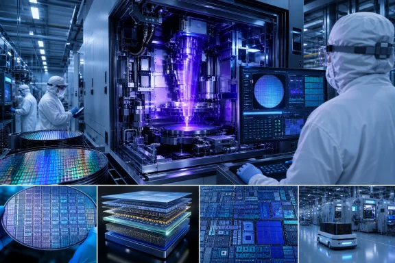
Intel Foundry says it has begun shipping a subset of Intel Core Ultra Series 3 “Panther Lake” processors made with ASML’s High NA EUV lithography on selected Intel 18A layers—the first claimed high-volume commercial logic shipment using the next generation of EUV tools. As reported by Interesting Engineering and detailed in ASML’s July 15 announcement, the milestone matters less as a sudden upgrade for a new laptop buyer and more as a real-world manufacturing test of a technology Intel will need for future process nodes.
The immediate practical takeaway is deliberately narrow. These are not entirely “High NA-made” processors, and Intel is not replacing its existing EUV production fleet for Panther Lake. The company is applying High NA EUV to particular layers within a subset of chips while its established ASML NXE EUV scanners continue to carry production volume. That distinction is crucial: Intel is placing the new equipment into a shipping product flow without betting the entire Core Ultra Series 3 ramp on a still-maturing manufacturing platform.
ASML said the relevant Intel 18A layers are now dual-qualified in Oregon, with product shipping at yields matching the existing NXE platform. That is a stronger statement than a lab demonstration, but it is still a qualification milestone rather than evidence that every Panther Lake SKU or layer has moved to the new scanner generation.
For Windows users, there is no High NA EUV toggle, driver feature, or revised Windows 11 requirement attached to this news. A Core Ultra Series 3 laptop purchased earlier this year may already contain a Panther Lake processor made on Intel 18A, but Intel has not identified which retail models or processor batches use High NA-patterned layers.
That is because lithography is a factory technology, not a consumer-facing platform feature. It is the process of projecting extremely fine circuit patterns onto silicon wafers. Better resolution and process control can eventually support denser transistors, improved power efficiency, and more capable designs, but those outcomes depend on the complete chip architecture, packaging, software, cooling configuration, and product binning—not simply on one exposure tool.
Intel launched Core Ultra Series 3 at CES in January 2026 as its first major AI PC platform built on the Intel 18A process. Systems began reaching global availability on January 27, and Intel later expanded the family with mainstream Intel Core Series 3 parts for commercial PCs, value laptops, and edge devices. The High NA announcement therefore lands during an active product cycle, rather than being attached to a distant prototype.
Reuters characterized the deployment as a way for Intel to learn how to run the equipment effectively on a portion of flagship Panther Lake laptop chips. That is the right way to read it. The company gets meaningful production data—on setup, uptime, overlay control, defect behavior, mask handling, and yield—while keeping the bulk of the process on hardware with a longer operating history.
That is why High NA has been closely watched but slowly deployed. A scanner is not useful in isolation; it must operate reliably as part of a full production line while achieving acceptable throughput and yield. Reuters reported that the new equipment costs roughly $400 million per tool, around twice the price of a standard EUV system, making the economic case as important as the imaging capability.
ASML’s language reflects this reality. The company says Intel’s selected-layer use will supply data to refine system setup, uptime, and manufacturing implementation before broader deployment. In other words, Intel is not announcing that High NA has solved the cost, cycle-time, or process-integration challenges of leading-edge manufacturing. It is demonstrating that the technology can participate in a commercial shipment without disrupting the established Intel 18A process flow.
For Intel Foundry, that is a strategically useful claim. The company has spent years trying to restore confidence in its process roadmap, with Intel 18A serving as the central proof point for both its own products and prospective foundry customers. Shipping Panther Lake in volume was already a critical test; using selected production layers to validate an even newer toolchain gives Intel a potentially valuable head start on the next transition.
Those facts matter because Panther Lake is not likely to be the end state for High NA in Intel’s roadmap. Intel 18A was designed around its existing manufacturing approach, and the current deployment is limited to selected layers. The deeper value is in proving a path toward later nodes where the trade-offs could be more favorable and where the industry will need increasingly precise patterning.
Tom’s Hardware recently reported that Intel expects Intel 14A risk production in 2028 and volume production in 2029, with High NA compatibility planned for select layers. Those dates remain far enough away that they should be treated as roadmap targets, not a promise that every part of the High NA ecosystem is ready today. But Intel’s decision to bring the tool into Panther Lake shipments gives its process teams several years of operational experience before 14A must carry a broad commercial load.
The competitive implication is equally important. Intel is establishing itself as the first company willing to use High NA EUV in a high-volume logic product, even if the implementation is selective. That may create useful institutional knowledge across fab operations, process control, and design enablement. It does not automatically mean Intel’s next chips will outperform rival products, nor does it establish a permanent manufacturing lead over TSMC or Samsung.
It may, however, become a signal worth tracking for organizations with long hardware-refresh cycles or supply-chain interests. Intel’s ability to carry a new lithography platform from R&D into repeatable high-volume output will influence the company’s capacity to deliver future client, edge, and data-center products on schedule. The company’s assertion that High NA-patterned layers match NXE yields is encouraging, but the meaningful tests are sustained output, tool availability, defect control, and economics over multiple product generations.
For now, Intel has turned High NA EUV from an advanced-fab demonstration into part of a commercial shipping flow. The next milestone is not another marketing label on Panther Lake laptops; it is whether Intel can expand that limited use without compromising cost or supply, then carry the lessons into Intel 14A and whatever comes after it.
The immediate practical takeaway is deliberately narrow. These are not entirely “High NA-made” processors, and Intel is not replacing its existing EUV production fleet for Panther Lake. The company is applying High NA EUV to particular layers within a subset of chips while its established ASML NXE EUV scanners continue to carry production volume. That distinction is crucial: Intel is placing the new equipment into a shipping product flow without betting the entire Core Ultra Series 3 ramp on a still-maturing manufacturing platform.
ASML said the relevant Intel 18A layers are now dual-qualified in Oregon, with product shipping at yields matching the existing NXE platform. That is a stronger statement than a lab demonstration, but it is still a qualification milestone rather than evidence that every Panther Lake SKU or layer has moved to the new scanner generation.
 A production foothold, not a new CPU feature
For Windows users, there is no High NA EUV toggle, driver feature, or revised Windows 11 requirement attached to this news. A Core Ultra Series 3 laptop purchased earlier this year may already contain a Panther Lake processor made on Intel 18A, but Intel has not identified which retail models or processor batches use High NA-patterned layers.That is because lithography is a factory technology, not a consumer-facing platform feature. It is the process of projecting extremely fine circuit patterns onto silicon wafers. Better resolution and process control can eventually support denser transistors, improved power efficiency, and more capable designs, but those outcomes depend on the complete chip architecture, packaging, software, cooling configuration, and product binning—not simply on one exposure tool.
Intel launched Core Ultra Series 3 at CES in January 2026 as its first major AI PC platform built on the Intel 18A process. Systems began reaching global availability on January 27, and Intel later expanded the family with mainstream Intel Core Series 3 parts for commercial PCs, value laptops, and edge devices. The High NA announcement therefore lands during an active product cycle, rather than being attached to a distant prototype.
Reuters characterized the deployment as a way for Intel to learn how to run the equipment effectively on a portion of flagship Panther Lake laptop chips. That is the right way to read it. The company gets meaningful production data—on setup, uptime, overlay control, defect behavior, mask handling, and yield—while keeping the bulk of the process on hardware with a longer operating history.
The manufacturing risk Intel is choosing to absorb
Conventional EUV already represented a major industry transition. High NA EUV raises the numerical aperture of the optical system, allowing finer patterning and tighter control at advanced geometries. In theory, that can reduce the complexity of some multi-patterning steps and create room for future density scaling. In practice, it introduces new dependencies across photoresists, masks, pellicles, metrology, computational lithography, process recipes, and wafer handling.That is why High NA has been closely watched but slowly deployed. A scanner is not useful in isolation; it must operate reliably as part of a full production line while achieving acceptable throughput and yield. Reuters reported that the new equipment costs roughly $400 million per tool, around twice the price of a standard EUV system, making the economic case as important as the imaging capability.
ASML’s language reflects this reality. The company says Intel’s selected-layer use will supply data to refine system setup, uptime, and manufacturing implementation before broader deployment. In other words, Intel is not announcing that High NA has solved the cost, cycle-time, or process-integration challenges of leading-edge manufacturing. It is demonstrating that the technology can participate in a commercial shipment without disrupting the established Intel 18A process flow.
For Intel Foundry, that is a strategically useful claim. The company has spent years trying to restore confidence in its process roadmap, with Intel 18A serving as the central proof point for both its own products and prospective foundry customers. Shipping Panther Lake in volume was already a critical test; using selected production layers to validate an even newer toolchain gives Intel a potentially valuable head start on the next transition.
Panther Lake is the vehicle, but 14A is the larger prize
ASML said Intel installed the industry’s first commercial High NA EUV system at its Hillsboro, Oregon R&D site in 2024. Intel also became the first company to install and complete acceptance testing for ASML’s second-generation TWINSCAN EXE:5200B, which ASML says improves throughput, overlay accuracy, and light-source capability over the earlier EXE:5000 system.Those facts matter because Panther Lake is not likely to be the end state for High NA in Intel’s roadmap. Intel 18A was designed around its existing manufacturing approach, and the current deployment is limited to selected layers. The deeper value is in proving a path toward later nodes where the trade-offs could be more favorable and where the industry will need increasingly precise patterning.
Tom’s Hardware recently reported that Intel expects Intel 14A risk production in 2028 and volume production in 2029, with High NA compatibility planned for select layers. Those dates remain far enough away that they should be treated as roadmap targets, not a promise that every part of the High NA ecosystem is ready today. But Intel’s decision to bring the tool into Panther Lake shipments gives its process teams several years of operational experience before 14A must carry a broad commercial load.
The competitive implication is equally important. Intel is establishing itself as the first company willing to use High NA EUV in a high-volume logic product, even if the implementation is selective. That may create useful institutional knowledge across fab operations, process control, and design enablement. It does not automatically mean Intel’s next chips will outperform rival products, nor does it establish a permanent manufacturing lead over TSMC or Samsung.
Why enterprise buyers should keep the claim in proportion
IT departments evaluating a Panther Lake Windows fleet should still use the ordinary procurement criteria: OEM support, BIOS and driver maturity, Windows 11 compatibility, manageability features, battery-life results in the intended chassis, application performance, security controls, and pricing. High NA EUV is not yet a practical differentiator among laptops on a purchase order.It may, however, become a signal worth tracking for organizations with long hardware-refresh cycles or supply-chain interests. Intel’s ability to carry a new lithography platform from R&D into repeatable high-volume output will influence the company’s capacity to deliver future client, edge, and data-center products on schedule. The company’s assertion that High NA-patterned layers match NXE yields is encouraging, but the meaningful tests are sustained output, tool availability, defect control, and economics over multiple product generations.
For now, Intel has turned High NA EUV from an advanced-fab demonstration into part of a commercial shipping flow. The next milestone is not another marketing label on Panther Lake laptops; it is whether Intel can expand that limited use without compromising cost or supply, then carry the lessons into Intel 14A and whatever comes after it.
References
- Primary source: Interesting Engineering
Published: 2026-07-15T22:45:57+00:00
Intel ships first commercial chips built with next-gen lithography
Intel becomes first to ship high-volume chips made with High Numerical Aperture EUV manufacturing technology.interestingengineering.com - Related coverage: tomshardware.com
Intel becomes the first company to ship high-volume logic chips made with ASML's High NA EUV — select Panther Lake layers on 18A are now dual-qualified for 0.55 NA scanners | Tom's Hardware
Milestone marks the technology's transition from R&D to full commercial deploymentwww.tomshardware.com - Related coverage: newsroom.intel.com
- Related coverage: pcgamer.com
Intel promises 'leadership across the board on desktop' when its next-gen Nova Lake CPU launches in late 2026 | PC Gamer
Beating AMD will be a tall order, but maybe 52 cores will do it.www.pcgamer.com
