

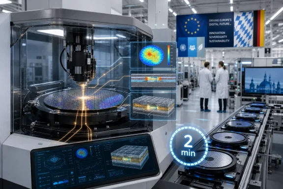
QuantumDiamonds, a Technical University of Munich spinout, said on July 8, 2026, that it has secured €76 million in non-dilutive backing from Germany and Bavaria to build semiconductor testing equipment in Munich, alongside a €15 million equity round led by World Fund. The practical news is this: QuantumDiamonds is shipping a lab-focused system today for R&D and failure analysis, while it is still developing the higher-throughput fab-floor system that would move the company closer to production-wide yield monitoring. Its headline claim is that diamond-based quantum sensing can reduce some chip-defect investigations from weeks to a two-minute inspection. If that claim holds up in customer environments, the company could become an important supplier of inspection and metrology tools for advanced semiconductor manufacturing. If it does not scale beyond specialist use cases, the story remains a promising but narrower deep-tech bet.
Europe’s semiconductor policy is often discussed in terms of fabs: where chips are made, who controls capacity, and how much public money is needed to reduce dependency on overseas manufacturing. That focus makes sense, but fabs are only one part of the semiconductor stack. The companies that make lithography tools, inspection systems, materials, design software, and process-control equipment can hold leverage even when they are not manufacturing the chips themselves.
QuantumDiamonds matters because it sits in one of those less visible layers: inspection and metrology. The chip industry is not merely trying to make more wafers; it is trying to understand why increasingly complex devices fail, where microscopic defects hide, and how to stop wasting value after expensive processing steps. In that world, a tool that finds hidden electrical failures can be strategically important even if it never prints a circuit or packages a chip.
TechCrunch reported that QuantumDiamonds has been granted €76 million in non-dilutive funding, provided by Germany’s federal economy ministry and the state of Bavaria, after approval by the European Commission. The startup plans to use the money to establish a Munich facility for production of semiconductor testing equipment. Separately, the company has raised a €15 million equity round led by World Fund, with Bayern Kapital and existing investors Creator Fund, Earlybird, First Momentum, IQ Capital, Onsight Ventures, and UnternehmerTUM also backing the round.
That split is important. The public backing is tied to building industrial capacity in Munich. The equity round signals that private investors believe the company can sell into the global semiconductor market. Put simply: the state is helping make the manufacturing base possible, while venture capital is underwriting the commercial expansion.
The Munich location is also part of the story. QuantumDiamonds is based there, most of its roughly 70-person team is there, and CEO Kevin Berghoff and co-founder and CTO Fleming Bruckmaier plan to expand the engineering organization. Berghoff’s point to TechCrunch was direct: the company believes it has what it needs in Munich to ship overseas.
That is the more concrete takeaway for readers. This is not just “Europe funds quantum.” It is a Munich semiconductor-equipment startup trying to convert university-origin technology into inspection tools that chipmakers and analysis labs can actually use.
QuantumDiamonds’ claim is that its synthetic diamonds can reveal what ordinary inspection methods may miss. The company uses properties of those diamonds to observe how electricity is flowing through chips. Instead of looking only at the surface, the system is presented as a way to detect defects through layers without destroying the chip.
That last point matters. Failure analysis in advanced semiconductors can be slow, invasive, and expensive. If engineers need to cut into a package, remove layers, or perform destructive preparation, the process can take time and may alter the evidence they are trying to examine. A non-destructive tool that can locate electrical failures inside a layered package would give engineers a better chance to debug the device as it actually exists.
TechCrunch reported QuantumDiamonds’ claim that it can compress a defect-detection process that often takes weeks into a two-minute inspection that does not stop production lines. The company also claims the technology can save large semiconductor customers hundreds of millions of dollars. Those savings should be treated as company claims rather than established industry-wide results. The economic logic is understandable, however: if a manufacturer can identify a yield problem earlier, it may waste fewer wafers, shorten root-cause analysis, and fix process issues before more value is lost.
This is especially relevant because the most expensive chips are not simple commodity parts. AI accelerators, high-end memory, advanced mobile processors, automotive electronics, and other complex devices depend on costly process flows and packaging. Every yield point matters. A tool that can show where current is not flowing properly, or where it is flowing when it should not, is not merely a science instrument. It can become a production-economics tool if it helps engineers act faster.
QuantumDiamonds’ current product positioning reflects that transition. Its current in-lab system is commercially available for R&D and failure analysis. Its in-line, high-throughput wafer-mapping system remains under development. In other words, the company has moved beyond academic proof-of-concept, but the harder move into routine fab-floor process control is still ahead.
That transition is the story.
For years, “quantum” has been one of the tech industry’s most elastic words. It can mean a near-term sensing instrument, a research-stage computer, a cryptography concern, a funding category, or a public-sector industrial policy slogan. In QuantumDiamonds’ case, the relevant point is not that some future quantum computer might solve a problem. It is that quantum sensing is being applied to a present manufacturing problem: finding hidden electrical defects in chips.
Customers do not buy mystery. They buy yield, speed, and less destructive analysis. If the system works, the synthetic diamond is simply the component that makes the measurement possible.
That distinction matters for IT and enterprise readers because it separates two very different kinds of “quantum” announcements. One kind asks buyers to prepare for a speculative future. The other appears quietly inside the hardware supply chain and may affect the cost, reliability, or availability of conventional computing equipment. QuantumDiamonds belongs in the second category.
It also helps explain why semiconductor customers would consider expensive tools. Berghoff told TechCrunch that the lab tools are priced in the single-digit millions, while a high-throughput system could reach $10 million to $15 million. In isolation, that is expensive. In semiconductor manufacturing, the relevant question is whether the tool pays for itself by improving yield, shortening failure analysis, or preventing repeated process errors. Any payback period should be treated as case-specific unless a customer publicly validates it.
The business model is not only the hardware sale. QuantumDiamonds also charges for on-site support and software that interprets data and gives clients a clearer indication of what to address in their manufacturing process. That makes the company less like a one-off instrument vendor and more like a process-intelligence supplier embedded in the customer’s engineering workflow.
For chipmakers, that software layer may matter as much as the sensor. A tool that produces unusual measurements but cannot help process engineers decide what to do next is a science project. A tool that maps hidden electrical failures into actionable production fixes is infrastructure.
That quote is the hinge of the story. The company’s current lab tool helps customers analyze failures and conduct R&D. The planned high-throughput system is aimed at a much bigger prize: broader quality control inside the fab. The “100% quality control” language is an ambition stated by the company, not proof that the industry has already adopted the system at that scale.
The table also shows why the story should not be overhyped. QuantumDiamonds has a commercially available lab system, but the full fab-wide quality-control vision remains a target. The company is out of the lab in the sense that it has a product for customer environments. It is not yet at the point where its most ambitious manufacturing vision should be treated as completed fact.
That nuance matters. Semiconductor fabs are conservative for good reason. Tools must survive uptime requirements, contamination controls, automation demands, data-security expectations, and procurement scrutiny. A lab system can be impressive and still face a difficult road to becoming a high-volume manufacturing tool if it is too slow, too delicate, too hard to integrate, or too difficult to interpret consistently.
QuantumDiamonds appears to understand that the prize is not a beautiful scan; it is throughput and actionability. The company’s current-versus-future product split makes that clear. Today’s tool is for R&D and failure analysis. The system under development is aimed at high-throughput wafer mapping, yield monitoring, and production-process optimization.
Those are different buying decisions. A lab may purchase a specialized tool because it improves root-cause analysis. A fab will demand evidence that the tool can fit into production workflows and justify its cost against existing inspection and metrology methods.
Current product status — QuantumDiamonds’ in-lab system is commercially available for R&D and failure analysis.
Next product target — QuantumDiamonds is developing an in-line, high-throughput wafer-mapping system aimed at broader yield monitoring and production-process optimization.
Still, the comparison is not random. ASML’s importance comes from owning a bottleneck. If a company controls a critical tool without which leading-edge manufacturing cannot efficiently proceed, it can gain leverage far beyond its revenue line. Europe’s semiconductor position is not defined only by how many chips it makes, but also by whether it controls indispensable equipment, materials, software, and process knowledge.
QuantumDiamonds is trying to become important in a different part of the stack. It does not print chip patterns. It tries to reveal hidden defects in chips whose complexity is outpacing some inspection methods. If advanced packaging and layered architectures continue to increase the difficulty of failure analysis, then tools that see through those layers could become more valuable.
The risk in the ASML comparison is that it can make a young company sound more proven than it is. ASML’s position was built over decades, through deep customer relationships, enormous engineering investment, and an ecosystem that is very difficult to replicate. QuantumDiamonds still has to prove that its technology can move from valuable lab use into broader manufacturing adoption.
There is also a competitive reality. Semiconductor-equipment incumbents have field-service networks, process-integration experience, procurement relationships, and the balance sheets to attack adjacent markets. If QuantumDiamonds’ technology becomes obviously valuable, larger companies will notice.
The company’s defense is speed and specialization. It is not trying to be a general inspection conglomerate. It is trying to own a specific measurement capability at a moment when chip architecture is making hidden electrical defects harder to find.
That is enough to make the company worth watching. It is not enough to declare it Europe’s next unavoidable semiconductor champion.
The Munich facility is therefore more than a real-estate detail. For a semiconductor-equipment company, production, application engineering, software, support, and customer demonstrations can reinforce one another. A production site for inspection and metrology tools can anchor engineers, suppliers, customer specialists, and research relationships. Even if the tools are sold overseas, the know-how and high-value work can remain concentrated in Munich.
The talent story is also central. QuantumDiamonds has a team of roughly 70 people, with most of them based in Munich, and the company plans to expand its engineering team. In deep tech, headcount growth is not just an HR metric; it is an execution risk. Scaling production tools requires mechanical engineering, photonics, quantum-sensing expertise, semiconductor-process knowledge, software, field support, and customer application engineering.
Europe often complains that it has science but struggles with scale. QuantumDiamonds is a test of whether that cliché can be broken in a narrow, valuable market. The company comes from the Technical University of Munich, has German and Bavarian backing, has venture support from World Fund and other investors, and is aiming at semiconductor customers beyond its home market.
That is the concrete policy takeaway. The most useful European semiconductor plays may not all be fabs. Some may be specialized toolmakers that strengthen the manufacturing chain from a more targeted position.
The comparison to other European quantum companies is useful only up to a point. QuantumDiamonds is not primarily asking customers to buy into a future quantum-computing roadmap. It is selling a sensing tool for a current semiconductor pain point. That may give it a more direct path to industrial revenue than more speculative quantum categories, provided customers validate the claimed speed, cost, and workflow benefits.
The diamond is not the product. The avoided yield loss is the product.
The direct action for admins is not to buy a QuantumDiamonds tool. Most enterprises will never see one. The relevance is procurement intelligence. As systems become more dependent on advanced packaging, chiplets, stacked memory, and dense accelerator designs, hardware validation becomes more important.
For IT teams, the practical question is not whether a supplier uses a particular quantum-sensing tool. The practical question is whether the supplier can explain how it validates advanced silicon packages, monitors quality, handles failure analysis, and manages first-generation platform risk.
That matters for AI PCs and GPU workstations because those categories often arrive with new silicon, new firmware, new drivers, new thermal behavior, and new platform assumptions. It matters even more for dense server deployments, where a hardware flaw can become a fleet problem quickly. Better inspection and failure analysis upstream can help vendors identify issues earlier, but enterprise buyers should still demand evidence at the product level.
Procurement teams should be especially careful with claims around “AI-ready” hardware, advanced accelerators, and high-bandwidth memory platforms. These systems may offer real performance advantages, but they also concentrate risk in packaging, thermals, firmware, drivers, and validation pipelines. A supplier that can explain its testing process is more credible than one that only lists benchmark numbers.
There is also a vendor-validation angle. If semiconductor manufacturers and analysis labs adopt faster non-destructive inspection, IT buyers may eventually see better root-cause analysis when hardware problems appear. That does not mean every device becomes flawless. It means suppliers may have better tools to diagnose problems before they spread into large production runs.
For Windows environments, the operational lesson is simple: hardware quality is now a software-reliability issue too. Driver crashes, firmware updates, thermal throttling, unstable accelerators, memory errors, and platform-specific bugs often look like IT problems by the time they reach the admin. Some of those issues begin much earlier in the silicon and packaging pipeline.
Those are company claims and commercial assumptions, not guaranteed customer outcomes. The actual business case will depend on the use case, the chip type, the defect mode, the tool’s throughput, and the customer’s existing inspection workflow. A two-minute inspection is compelling only if it produces reliable, actionable results at the right point in the process.
That is the kind of equation semiconductor executives understand. They do not need to believe in quantum as a movement. They need to believe that the tool reduces scrap, accelerates root-cause analysis, and helps engineers fix processes before the same defect repeats across more expensive production.
The risk is that the most compelling economics may depend on use cases where QuantumDiamonds is not yet fully deployed. Lab failure analysis is valuable, but the larger upside comes from moving toward high-throughput fab quality control. That requires performance at production scale.
It also requires trust. A fab will not insert a novel tool into its workflow simply because it is elegant. It must integrate with existing inspection, metrology, manufacturing execution systems, data pipelines, and engineering procedures. It must be maintained. It must produce repeatable results. It must earn its place against incumbent approaches, even if those approaches are slower or more destructive.
QuantumDiamonds’ early commercial traction and customer conversations therefore matter more than the funding number. Public money can help build capacity. Venture money can extend runway. Neither proves that a tool will become standard in fabs. The proof will come from repeat purchases, production integration, and customer-validated improvements in analysis speed, yield learning, or defect detection.
The company’s story should be understood in stages. Stage one is a commercially available lab system for R&D and failure analysis. Stage two is wider use by semiconductor labs and manufacturers that need non-destructive insight into complex packages. Stage three, still ahead, is high-throughput fab-floor adoption. Each stage has a different risk profile.
That staged view is more useful than either hype or dismissal. QuantumDiamonds does not need to become ASML to matter. A specialized toolmaker that improves advanced failure analysis could still be a meaningful company. But if it does succeed in turning diamond-based sensing into a production-control layer for advanced chips, the upside becomes much larger.
First, watch whether QuantumDiamonds can convert the €76 million non-dilutive backing into a Munich facility that actually scales production of semiconductor testing equipment. Facility announcements are easy to understand but hard to execute. Hiring, supply chains, manufacturing quality, customer support, and process repeatability will determine whether the funding becomes industrial capacity.
Second, watch whether the €15 million equity round helps the company expand commercially without pulling it away from its core technical problem. Deep-tech startups often face pressure to tell a broader story than their product can support. QuantumDiamonds’ strongest story is narrow and concrete: faster, non-destructive electrical defect inspection for complex chips.
Third, watch the current-versus-future product split. The commercially available lab system is the present business. The high-throughput wafer-mapping system is the bigger ambition. Readers should be cautious when those two are blended together. A tool that works well for R&D and failure analysis is not automatically a fab-wide quality-control platform.
Fourth, watch customer validation. The company’s savings claims, two-minute inspection pitch, and 100% quality-control ambition become much more persuasive when customers describe their own results. Until then, they should be treated as claims from the company and its investors.
Fifth, watch how incumbents respond. If established semiconductor-equipment companies ignore the category, that may say something about market size or technical difficulty. If they partner, acquire, or build competing approaches, that may validate the importance of the measurement problem even if QuantumDiamonds does not capture the entire market.
The cleanest way to summarize the story is this: QuantumDiamonds has money, a Munich manufacturing plan, a commercial lab product, and a large claim about inspection speed. What it does not yet have, at least based on the verified facts available here, is proven industry-wide deployment of its future high-throughput vision.
That makes the company interesting rather than inevitable.
If Europe cannot own every fab, it can still own tools, materials, measurement systems, design capabilities, and process knowledge that the global chip industry needs. QuantumDiamonds is attempting to occupy one of those positions: non-destructive electrical inspection for chips that are increasingly difficult to understand from the outside.
The July 8, 2026 news gives the company more capital and a stronger industrial base. It does not remove the execution risk. The company still has to scale manufacturing, support customers, prove repeatability, compete with larger inspection players, and bridge the gap between lab analysis and high-throughput fab use.
For Windows users and IT buyers, the story is a reminder that the reliability of modern computing does not begin with the operating system. It begins in design, fabrication, packaging, inspection, validation, firmware, drivers, and support. By the time a device reaches a desk or a rack, thousands of upstream decisions have already shaped its reliability.
QuantumDiamonds is working far upstream in that chain. If its tools help chipmakers find hidden defects faster, the effects may eventually show up as better validated hardware, fewer production surprises, and more confidence in advanced silicon platforms. If the technology remains confined to narrower lab use, it may still be valuable, just less transformational.
Either outcome is worth watching. The company has a specific tool, a specific facility plan, a specific funding package, and a specific customer problem. In a semiconductor market crowded with abstractions, that concreteness is the strongest part of the story.
 Europe’s chip strategy finally finds a wedge that is not another fab
Europe’s semiconductor policy is often discussed in terms of fabs: where chips are made, who controls capacity, and how much public money is needed to reduce dependency on overseas manufacturing. That focus makes sense, but fabs are only one part of the semiconductor stack. The companies that make lithography tools, inspection systems, materials, design software, and process-control equipment can hold leverage even when they are not manufacturing the chips themselves.QuantumDiamonds matters because it sits in one of those less visible layers: inspection and metrology. The chip industry is not merely trying to make more wafers; it is trying to understand why increasingly complex devices fail, where microscopic defects hide, and how to stop wasting value after expensive processing steps. In that world, a tool that finds hidden electrical failures can be strategically important even if it never prints a circuit or packages a chip.
TechCrunch reported that QuantumDiamonds has been granted €76 million in non-dilutive funding, provided by Germany’s federal economy ministry and the state of Bavaria, after approval by the European Commission. The startup plans to use the money to establish a Munich facility for production of semiconductor testing equipment. Separately, the company has raised a €15 million equity round led by World Fund, with Bayern Kapital and existing investors Creator Fund, Earlybird, First Momentum, IQ Capital, Onsight Ventures, and UnternehmerTUM also backing the round.
That split is important. The public backing is tied to building industrial capacity in Munich. The equity round signals that private investors believe the company can sell into the global semiconductor market. Put simply: the state is helping make the manufacturing base possible, while venture capital is underwriting the commercial expansion.
The Munich location is also part of the story. QuantumDiamonds is based there, most of its roughly 70-person team is there, and CEO Kevin Berghoff and co-founder and CTO Fleming Bruckmaier plan to expand the engineering organization. Berghoff’s point to TechCrunch was direct: the company believes it has what it needs in Munich to ship overseas.
That is the more concrete takeaway for readers. This is not just “Europe funds quantum.” It is a Munich semiconductor-equipment startup trying to convert university-origin technology into inspection tools that chipmakers and analysis labs can actually use.
The real bottleneck is not making chips; it is knowing which ones are broken
The semiconductor industry’s problem is no longer only that transistors are hard to shrink. It is also that the devices built around them are getting harder to inspect, debug, and validate. Advanced packaging, chiplets, stacked memory, interposers, and 3D architectures increase the number of places where something can go wrong while making traditional inspection harder.QuantumDiamonds’ claim is that its synthetic diamonds can reveal what ordinary inspection methods may miss. The company uses properties of those diamonds to observe how electricity is flowing through chips. Instead of looking only at the surface, the system is presented as a way to detect defects through layers without destroying the chip.
That last point matters. Failure analysis in advanced semiconductors can be slow, invasive, and expensive. If engineers need to cut into a package, remove layers, or perform destructive preparation, the process can take time and may alter the evidence they are trying to examine. A non-destructive tool that can locate electrical failures inside a layered package would give engineers a better chance to debug the device as it actually exists.
TechCrunch reported QuantumDiamonds’ claim that it can compress a defect-detection process that often takes weeks into a two-minute inspection that does not stop production lines. The company also claims the technology can save large semiconductor customers hundreds of millions of dollars. Those savings should be treated as company claims rather than established industry-wide results. The economic logic is understandable, however: if a manufacturer can identify a yield problem earlier, it may waste fewer wafers, shorten root-cause analysis, and fix process issues before more value is lost.
This is especially relevant because the most expensive chips are not simple commodity parts. AI accelerators, high-end memory, advanced mobile processors, automotive electronics, and other complex devices depend on costly process flows and packaging. Every yield point matters. A tool that can show where current is not flowing properly, or where it is flowing when it should not, is not merely a science instrument. It can become a production-economics tool if it helps engineers act faster.
QuantumDiamonds’ current product positioning reflects that transition. Its current in-lab system is commercially available for R&D and failure analysis. Its in-line, high-throughput wafer-mapping system remains under development. In other words, the company has moved beyond academic proof-of-concept, but the harder move into routine fab-floor process control is still ahead.
That transition is the story.
Quantum is only useful here because the customer can ignore it
One of the most useful details in the TechCrunch interview is Berghoff’s admission that customers “couldn’t care less about it being quantum.” That is not a throwaway line. It is a sign that this is being sold as an industrial measurement tool, not as a quantum branding exercise.For years, “quantum” has been one of the tech industry’s most elastic words. It can mean a near-term sensing instrument, a research-stage computer, a cryptography concern, a funding category, or a public-sector industrial policy slogan. In QuantumDiamonds’ case, the relevant point is not that some future quantum computer might solve a problem. It is that quantum sensing is being applied to a present manufacturing problem: finding hidden electrical defects in chips.
Customers do not buy mystery. They buy yield, speed, and less destructive analysis. If the system works, the synthetic diamond is simply the component that makes the measurement possible.
That distinction matters for IT and enterprise readers because it separates two very different kinds of “quantum” announcements. One kind asks buyers to prepare for a speculative future. The other appears quietly inside the hardware supply chain and may affect the cost, reliability, or availability of conventional computing equipment. QuantumDiamonds belongs in the second category.
It also helps explain why semiconductor customers would consider expensive tools. Berghoff told TechCrunch that the lab tools are priced in the single-digit millions, while a high-throughput system could reach $10 million to $15 million. In isolation, that is expensive. In semiconductor manufacturing, the relevant question is whether the tool pays for itself by improving yield, shortening failure analysis, or preventing repeated process errors. Any payback period should be treated as case-specific unless a customer publicly validates it.
The business model is not only the hardware sale. QuantumDiamonds also charges for on-site support and software that interprets data and gives clients a clearer indication of what to address in their manufacturing process. That makes the company less like a one-off instrument vendor and more like a process-intelligence supplier embedded in the customer’s engineering workflow.
For chipmakers, that software layer may matter as much as the sensor. A tool that produces unusual measurements but cannot help process engineers decide what to do next is a science project. A tool that maps hidden electrical failures into actionable production fixes is infrastructure.
From sample-based lab work to 100 percent quality control
The gap between QuantumDiamonds’ current state and its ambition can be seen in Berghoff’s own description. “What we have now is a tool for a lab environment, where you do sample-based testing, and test maybe one out of a million chips,” he told TechCrunch. “What we now aim for is to also do high-throughput testing, meaning you can do 100% quality control in the fab itself.”That quote is the hinge of the story. The company’s current lab tool helps customers analyze failures and conduct R&D. The planned high-throughput system is aimed at a much bigger prize: broader quality control inside the fab. The “100% quality control” language is an ambition stated by the company, not proof that the industry has already adopted the system at that scale.
| Capability | Current lab tool | Future high-throughput system |
|---|---|---|
| Primary setting | Lab environment | Fab itself |
| Testing model | Sample-based testing | High-throughput testing |
| Sampling level described | “Maybe one out of a million chips,” according to Berghoff | Company target of 100% quality control |
| Price range described by company | Single-digit millions | Up to $10 million to $15 million |
| Customer value | R&D, failure analysis, and process insight | Yield monitoring and production-process optimization if successfully deployed at scale |
That nuance matters. Semiconductor fabs are conservative for good reason. Tools must survive uptime requirements, contamination controls, automation demands, data-security expectations, and procurement scrutiny. A lab system can be impressive and still face a difficult road to becoming a high-volume manufacturing tool if it is too slow, too delicate, too hard to integrate, or too difficult to interpret consistently.
QuantumDiamonds appears to understand that the prize is not a beautiful scan; it is throughput and actionability. The company’s current-versus-future product split makes that clear. Today’s tool is for R&D and failure analysis. The system under development is aimed at high-throughput wafer mapping, yield monitoring, and production-process optimization.
Those are different buying decisions. A lab may purchase a specialized tool because it improves root-cause analysis. A fab will demand evidence that the tool can fit into production workflows and justify its cost against existing inspection and metrology methods.
Timeline
July 8, 2026 — QuantumDiamonds said it had secured €76 million in non-dilutive backing from Germany and Bavaria for a Munich semiconductor-testing-equipment facility, alongside a €15 million equity round led by World Fund.Current product status — QuantumDiamonds’ in-lab system is commercially available for R&D and failure analysis.
Next product target — QuantumDiamonds is developing an in-line, high-throughput wafer-mapping system aimed at broader yield monitoring and production-process optimization.
The ASML comparison is flattering, dangerous, and not entirely absurd
World Fund managing partner Daria Saharova wrote that QuantumDiamonds “can become Europe’s next ASML.” That is venture capital language, and it should be read with the usual discount. ASML is not merely a successful European technology company; it is a near-irreplaceable supplier in one of the most important manufacturing chains in the world. Comparisons to ASML are usually more aspiration than analysis.Still, the comparison is not random. ASML’s importance comes from owning a bottleneck. If a company controls a critical tool without which leading-edge manufacturing cannot efficiently proceed, it can gain leverage far beyond its revenue line. Europe’s semiconductor position is not defined only by how many chips it makes, but also by whether it controls indispensable equipment, materials, software, and process knowledge.
QuantumDiamonds is trying to become important in a different part of the stack. It does not print chip patterns. It tries to reveal hidden defects in chips whose complexity is outpacing some inspection methods. If advanced packaging and layered architectures continue to increase the difficulty of failure analysis, then tools that see through those layers could become more valuable.
The risk in the ASML comparison is that it can make a young company sound more proven than it is. ASML’s position was built over decades, through deep customer relationships, enormous engineering investment, and an ecosystem that is very difficult to replicate. QuantumDiamonds still has to prove that its technology can move from valuable lab use into broader manufacturing adoption.
There is also a competitive reality. Semiconductor-equipment incumbents have field-service networks, process-integration experience, procurement relationships, and the balance sheets to attack adjacent markets. If QuantumDiamonds’ technology becomes obviously valuable, larger companies will notice.
The company’s defense is speed and specialization. It is not trying to be a general inspection conglomerate. It is trying to own a specific measurement capability at a moment when chip architecture is making hidden electrical defects harder to find.
That is enough to make the company worth watching. It is not enough to declare it Europe’s next unavoidable semiconductor champion.
Munich is being used as a launchpad, not a shelter
The most important industrial-policy detail in the story may be that QuantumDiamonds is not presenting European support as a way to serve only European customers. It is building in Munich while aiming at the global semiconductor market. That is the stronger version of European deep tech: keep high-value engineering and production capacity in Europe, but sell into the places where the most demanding customers operate.The Munich facility is therefore more than a real-estate detail. For a semiconductor-equipment company, production, application engineering, software, support, and customer demonstrations can reinforce one another. A production site for inspection and metrology tools can anchor engineers, suppliers, customer specialists, and research relationships. Even if the tools are sold overseas, the know-how and high-value work can remain concentrated in Munich.
The talent story is also central. QuantumDiamonds has a team of roughly 70 people, with most of them based in Munich, and the company plans to expand its engineering team. In deep tech, headcount growth is not just an HR metric; it is an execution risk. Scaling production tools requires mechanical engineering, photonics, quantum-sensing expertise, semiconductor-process knowledge, software, field support, and customer application engineering.
Europe often complains that it has science but struggles with scale. QuantumDiamonds is a test of whether that cliché can be broken in a narrow, valuable market. The company comes from the Technical University of Munich, has German and Bavarian backing, has venture support from World Fund and other investors, and is aiming at semiconductor customers beyond its home market.
That is the concrete policy takeaway. The most useful European semiconductor plays may not all be fabs. Some may be specialized toolmakers that strengthen the manufacturing chain from a more targeted position.
The comparison to other European quantum companies is useful only up to a point. QuantumDiamonds is not primarily asking customers to buy into a future quantum-computing roadmap. It is selling a sensing tool for a current semiconductor pain point. That may give it a more direct path to industrial revenue than more speculative quantum categories, provided customers validate the claimed speed, cost, and workflow benefits.
The diamond is not the product. The avoided yield loss is the product.
Why this matters to Windows users and enterprise IT
At first glance, a Munich semiconductor-inspection startup sounds far removed from WindowsForum’s usual universe of Windows updates, drivers, laptops, workstations, servers, and enterprise endpoints. It is not. This sits upstream of the hardware that Windows users and IT departments will buy: AI PCs, GPU workstations, storage controllers, networking hardware, servers, and high-end mobile workstations.The direct action for admins is not to buy a QuantumDiamonds tool. Most enterprises will never see one. The relevance is procurement intelligence. As systems become more dependent on advanced packaging, chiplets, stacked memory, and dense accelerator designs, hardware validation becomes more important.
For IT teams, the practical question is not whether a supplier uses a particular quantum-sensing tool. The practical question is whether the supplier can explain how it validates advanced silicon packages, monitors quality, handles failure analysis, and manages first-generation platform risk.
That matters for AI PCs and GPU workstations because those categories often arrive with new silicon, new firmware, new drivers, new thermal behavior, and new platform assumptions. It matters even more for dense server deployments, where a hardware flaw can become a fleet problem quickly. Better inspection and failure analysis upstream can help vendors identify issues earlier, but enterprise buyers should still demand evidence at the product level.
Procurement teams should be especially careful with claims around “AI-ready” hardware, advanced accelerators, and high-bandwidth memory platforms. These systems may offer real performance advantages, but they also concentrate risk in packaging, thermals, firmware, drivers, and validation pipelines. A supplier that can explain its testing process is more credible than one that only lists benchmark numbers.
There is also a vendor-validation angle. If semiconductor manufacturers and analysis labs adopt faster non-destructive inspection, IT buyers may eventually see better root-cause analysis when hardware problems appear. That does not mean every device becomes flawless. It means suppliers may have better tools to diagnose problems before they spread into large production runs.
For Windows environments, the operational lesson is simple: hardware quality is now a software-reliability issue too. Driver crashes, firmware updates, thermal throttling, unstable accelerators, memory errors, and platform-specific bugs often look like IT problems by the time they reach the admin. Some of those issues begin much earlier in the silicon and packaging pipeline.
Action checklist for admins
- Treat advanced silicon reliability as a procurement topic for AI PCs, GPU workstations, edge-inference systems, and high-density servers.
- Ask hardware suppliers how they validate advanced packaging, memory stacks, chiplet-based designs, and accelerator modules before fleet-scale rollout.
- Request evidence of failure-analysis maturity, not just marketing language about performance or AI capability.
- For critical deployments, demand pilot batches, burn-in data, firmware maturity details, and support commitments before committing to large purchases of first-generation platforms.
- Include packaging complexity, thermal design, driver maturity, and vendor validation practices in risk reviews for long-lived infrastructure buys.
- Track whether suppliers can explain how they monitor yield, identify defects, and respond when hardware issues appear in the field.
- For AI hardware procurement, compare vendors on supportability and validation transparency as well as raw TOPS, GPU performance, or benchmark claims.
The business case rests on speed, not elegance
The strongest part of QuantumDiamonds’ story is that its claimed value proposition is simple. A process that can take weeks becomes a two-minute inspection. A lab tool priced in the single-digit millions, or a future high-throughput system priced as high as $10 million to $15 million, may be attractive if it prevents enough yield loss or shortens root-cause analysis. Software and on-site support are meant to turn raw measurement into process advice.Those are company claims and commercial assumptions, not guaranteed customer outcomes. The actual business case will depend on the use case, the chip type, the defect mode, the tool’s throughput, and the customer’s existing inspection workflow. A two-minute inspection is compelling only if it produces reliable, actionable results at the right point in the process.
That is the kind of equation semiconductor executives understand. They do not need to believe in quantum as a movement. They need to believe that the tool reduces scrap, accelerates root-cause analysis, and helps engineers fix processes before the same defect repeats across more expensive production.
The risk is that the most compelling economics may depend on use cases where QuantumDiamonds is not yet fully deployed. Lab failure analysis is valuable, but the larger upside comes from moving toward high-throughput fab quality control. That requires performance at production scale.
It also requires trust. A fab will not insert a novel tool into its workflow simply because it is elegant. It must integrate with existing inspection, metrology, manufacturing execution systems, data pipelines, and engineering procedures. It must be maintained. It must produce repeatable results. It must earn its place against incumbent approaches, even if those approaches are slower or more destructive.
QuantumDiamonds’ early commercial traction and customer conversations therefore matter more than the funding number. Public money can help build capacity. Venture money can extend runway. Neither proves that a tool will become standard in fabs. The proof will come from repeat purchases, production integration, and customer-validated improvements in analysis speed, yield learning, or defect detection.
The company’s story should be understood in stages. Stage one is a commercially available lab system for R&D and failure analysis. Stage two is wider use by semiconductor labs and manufacturers that need non-destructive insight into complex packages. Stage three, still ahead, is high-throughput fab-floor adoption. Each stage has a different risk profile.
That staged view is more useful than either hype or dismissal. QuantumDiamonds does not need to become ASML to matter. A specialized toolmaker that improves advanced failure analysis could still be a meaningful company. But if it does succeed in turning diamond-based sensing into a production-control layer for advanced chips, the upside becomes much larger.
What to watch next
The next proof points are practical, not poetic.First, watch whether QuantumDiamonds can convert the €76 million non-dilutive backing into a Munich facility that actually scales production of semiconductor testing equipment. Facility announcements are easy to understand but hard to execute. Hiring, supply chains, manufacturing quality, customer support, and process repeatability will determine whether the funding becomes industrial capacity.
Second, watch whether the €15 million equity round helps the company expand commercially without pulling it away from its core technical problem. Deep-tech startups often face pressure to tell a broader story than their product can support. QuantumDiamonds’ strongest story is narrow and concrete: faster, non-destructive electrical defect inspection for complex chips.
Third, watch the current-versus-future product split. The commercially available lab system is the present business. The high-throughput wafer-mapping system is the bigger ambition. Readers should be cautious when those two are blended together. A tool that works well for R&D and failure analysis is not automatically a fab-wide quality-control platform.
Fourth, watch customer validation. The company’s savings claims, two-minute inspection pitch, and 100% quality-control ambition become much more persuasive when customers describe their own results. Until then, they should be treated as claims from the company and its investors.
Fifth, watch how incumbents respond. If established semiconductor-equipment companies ignore the category, that may say something about market size or technical difficulty. If they partner, acquire, or build competing approaches, that may validate the importance of the measurement problem even if QuantumDiamonds does not capture the entire market.
The cleanest way to summarize the story is this: QuantumDiamonds has money, a Munich manufacturing plan, a commercial lab product, and a large claim about inspection speed. What it does not yet have, at least based on the verified facts available here, is proven industry-wide deployment of its future high-throughput vision.
That makes the company interesting rather than inevitable.
Europe does not need every chip; it needs irreplaceable positions
The forward-looking lesson is not that Europe is about to dominate semiconductor manufacturing because one Munich startup raised money and won public backing. That would be the wrong conclusion. The better conclusion is that semiconductor leverage can come from targeted bottlenecks.If Europe cannot own every fab, it can still own tools, materials, measurement systems, design capabilities, and process knowledge that the global chip industry needs. QuantumDiamonds is attempting to occupy one of those positions: non-destructive electrical inspection for chips that are increasingly difficult to understand from the outside.
The July 8, 2026 news gives the company more capital and a stronger industrial base. It does not remove the execution risk. The company still has to scale manufacturing, support customers, prove repeatability, compete with larger inspection players, and bridge the gap between lab analysis and high-throughput fab use.
For Windows users and IT buyers, the story is a reminder that the reliability of modern computing does not begin with the operating system. It begins in design, fabrication, packaging, inspection, validation, firmware, drivers, and support. By the time a device reaches a desk or a rack, thousands of upstream decisions have already shaped its reliability.
QuantumDiamonds is working far upstream in that chain. If its tools help chipmakers find hidden defects faster, the effects may eventually show up as better validated hardware, fewer production surprises, and more confidence in advanced silicon platforms. If the technology remains confined to narrower lab use, it may still be valuable, just less transformational.
Either outcome is worth watching. The company has a specific tool, a specific facility plan, a specific funding package, and a specific customer problem. In a semiconductor market crowded with abstractions, that concreteness is the strongest part of the story.
References
- Primary source: TechCrunch
Published: Wed, 08 Jul 2026 20:29:50 GMT
Loading…
techcrunch.com - Related coverage: evertiq.com
Loading…
evertiq.com - Related coverage: quantumcomputingreport.com
Loading…
quantumcomputingreport.com - Related coverage: evertiq.es
Loading…
evertiq.es - Related coverage: evertiq.pl
Loading…
evertiq.pl - Related coverage: tomshardware.com
Loading…
www.tomshardware.com