

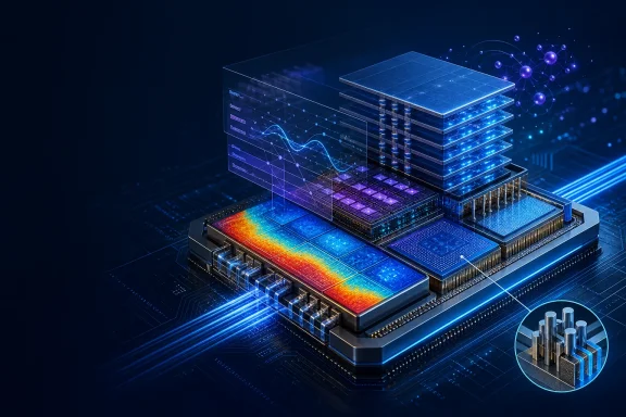
Semiconductor research published in the July 21 technical-paper roundup points to a computing industry reorganizing itself around three stubborn constraints: moving data costs too much energy, dense systems generate too much heat, and software can no longer remain tightly coupled to a single hardware configuration. The seven highlighted studies span custom high-bandwidth memory for large language models, processing-in-memory for 3D DRAM, software-defined vehicles, 3nm gate-all-around SRAM, monolithic electronic-photonic integration, room-temperature quantum photonics, and AI-assisted thermal analysis. Taken together, they suggest that the next major performance gains will come less from faster standalone processors and more from redesigning the interfaces between compute, memory, photonics, packaging, and software.
Semiconductor progress was once presented primarily as a transistor-scaling story. Smaller transistors enabled higher clock speeds, greater density, lower cost per function, and steadily more capable PCs without forcing software developers or system builders to rethink the entire machine.
That model has weakened. Leading-edge transistors continue to improve, but advanced systems increasingly run into bottlenecks outside the arithmetic units: memory bandwidth, data movement, interconnect latency, power delivery, heat extraction, packaging yield, and software portability. The July 21 roundup captures this transition unusually well because nearly every paper focuses on a boundary between traditionally separate domains.
The operating system increasingly sits above a heterogeneous collection of specialized engines rather than one general-purpose CPU. Research that changes where computation occurs also changes how Windows schedules work, manages memory, exposes devices, handles updates, enforces security, and reports failures.
Quantization reduces memory capacity and bandwidth requirements, but it does not make the conversion work disappear. Conventional systems may use GPU or accelerator cores to dequantize weights, consuming arithmetic resources and forcing additional data through an already congested memory hierarchy.
The researchers report up to a 7.08-times speedup and 90.23% lower energy consumption for the evaluated mixed-precision matrix-multiplication workloads. Those results should be treated as workload- and configuration-dependent rather than universal product guarantees, but they demonstrate the potential value of moving a narrowly defined operation to the point where the data already resides.
This is an example of near-memory processing rather than a wholesale replacement for GPUs. The proposed hardware does not attempt to execute an entire AI model inside HBM. It accelerates a recurring data transformation that otherwise consumes bandwidth, energy, and compute cycles.
That shift could strengthen memory vendors’ influence over system architecture. A memory supplier that offers hardware tailored to popular inference formats may deliver system-level benefits that cannot be measured by bandwidth specifications alone.
The likely adoption sequence would involve:
If managed well, the result could be faster local and cloud inference with no visible application change. If managed poorly, custom HBM features could fragment the ecosystem into vendor-specific execution paths that are difficult to optimize, test, and support.
The purpose is not simply to estimate storage behavior. The model is intended to explore processing-in-memory operations, including logic performed through coordinated activation of DRAM rows and sense-amplifier behavior.
A circuit-aware open model gives researchers a more consistent foundation for testing ideas. It can also make comparisons more meaningful by reducing reliance on proprietary assumptions that outside teams cannot inspect.
This matters because processing-in-memory has generated enthusiasm for years without becoming a universal computing model. The concept is compelling: if moving data to a processor consumes more energy than the operation itself, perform at least some operations where the data is stored. The difficulty lies in making those operations reliable, programmable, manufacturable, and useful across enough workloads.
This technique repurposes behavior already present in the memory array, but it also creates challenges. DRAM was designed to store data predictably, not to act as a general logic fabric. Retention characteristics, row disturbance, process variation, refresh operations, and error correction all influence whether such techniques can move from simulation into dependable products.
If practical manufacturing processes mature, vertically integrated memory could support more local parallelism and more tightly coupled processing-in-memory functions. However, thermal budgets become critical because upper device layers must be fabricated without damaging structures below them.
For Windows systems, PIM would raise questions extending from memory allocation to security. The operating system and hypervisor may eventually need to distinguish between ordinary memory regions and regions capable of executing approved operations, while preventing one tenant, process, or virtual machine from observing another’s data-dependent behavior.
Modern vehicles may contain dozens of electronic control units assembled from different processor families, real-time operating systems, buses, sensors, accelerators, and supplier-specific software stacks. Software-defined vehicles seek to consolidate functions, support over-the-air updates, and allow features to evolve throughout the vehicle’s service life.
Vehicles make the problem harder because many workloads have strict timing and safety requirements. A brake-control function cannot tolerate unpredictable latency merely because an abstraction layer makes software deployment more convenient. Infotainment, driver assistance, powertrain control, body electronics, and autonomous functions may also require very different assurance levels.
The Stuttgart team evaluates automotive HAL approaches alongside mechanisms from smartphones, networking, and industrial automation. That cross-domain comparison is valuable because other industries have already confronted hardware diversity, modular software, virtualization, and large-scale update management.
Automotive platforms face the same trade-off under more severe safety constraints. A durable HAL could let vehicle software migrate between processor generations, but it could also create a privileged layer whose defects affect many vehicle models.
A practical SDV architecture therefore needs several qualities:
The downside is that vehicles become persistent software platforms requiring patch governance similar to enterprise PCs. Unsupported firmware, expired certificates, incompatible updates, and supplier abandonment could become operational risks long before the mechanical vehicle reaches the end of its life.
Gate-all-around field-effect transistors use a gate that surrounds the channel more completely than earlier FinFET designs. This improves electrostatic control and supports continued scaling, but the geometry and isolation structures can impede heat flow.
That heat can alter mobility, delay, leakage, aging, and SRAM stability. Because SRAM arrays occupy substantial processor area and are sensitive to small voltage margins, local thermal effects can influence cache reliability and maximum operating frequency.
The paper compares a punch-through-stopper design with bottom-dielectric-isolation techniques. It also proposes a channel-focused BDI configuration that changes how the source and drain connect to the substrate. Each approach balances electrostatic control, thermal conduction, leakage, and radiation response differently.
The researchers report that the evaluated structures resisted alpha-particle-induced SRAM upsets under their tested conditions, while bottom dielectric isolation substantially improved radiation hardness. Those findings are encouraging, but they do not eliminate the need to test broader particle types, energies, operating voltages, cell layouts, and manufacturing variations.
Windows users may experience the consequences indirectly through boost behavior, corrected hardware-error logs, firmware updates, and platform-specific power profiles. A processor that protects itself by reducing frequency under a microscopic hotspot may appear to have an inconsistent performance problem unless diagnostic tools can explain the cause.
The significance lies in bringing photonic functions and their control electronics closer together. Photonic chips frequently require external drivers, digital-to-analog converters, calibration loops, and packaging connections. Those interfaces consume area and power while complicating manufacturing.
The demonstrated platform reportedly includes silicon-nitride waveguides, tunable ring resonators, and photonic digital-to-analog conversion capabilities integrated at wafer scale. Such a combination could be useful in communications, sensing, photonic AI, and quantum systems.
Monolithic integration differs from assembling separately fabricated electronic and photonic dies in a package. The monolithic route can shorten connections and improve density, although it also forces all structures to coexist within compatible process rules.
This means future photonic accelerators may require persistent control software rather than static configuration. Drivers may monitor optical channels, tune resonators, compensate for temperature drift, and retire degraded paths.
For Windows workstations or edge servers equipped with photonic accelerators, that control layer would likely resemble a mixture of a graphics driver, network driver, and hardware-management service. Its security and update quality would matter as much as raw optical performance.
Room-temperature operation is attractive because several leading quantum-computing approaches require extreme cooling. Photonic systems avoid some cryogenic constraints, although photon generation, detection, loss management, and error correction remain formidable challenges.
Photonic quantum processors could also connect naturally with optical communication systems. In principle, photons can carry quantum information between processors without the same electrical conversion steps required by non-photonic qubits.
However, the phrase room-temperature quantum processor should not be mistaken for a desktop quantum PC. Supporting lasers, photon sources, detectors, control electronics, packaging, and classical computation can still occupy substantial space and consume significant power.
The software flow could resemble current GPU and cloud-acceleration models:
The University of Florida-led paper combines AI-driven thermal modeling with a design-based heuristic method. The goal is to reconstruct and manage thermal behavior even when only sparse sensor data is available.
Simulation can fill the gaps, but high-fidelity multiphysics models are computationally expensive and depend on accurate material and boundary-condition data. Machine learning offers a potential middle ground by learning relationships between limited sensor measurements and a more complete thermal field.
The danger is false confidence. An AI model can generate a visually convincing temperature map while missing an operating condition not represented in its training data. Thermal-management systems therefore need uncertainty estimates, validation measurements, and safe fallback behavior.
Windows already supports thermal frameworks that coordinate firmware, device drivers, and operating-system power policy. Photonic and 3D-integrated devices would extend that model, potentially adding optical-health telemetry and predictive thermal controls.
For administrators, the result could be more efficient systems but more complicated diagnostics. A workload may slow not because the CPU or GPU is hot, but because a photonic interconnect layer has approached a calibration or reliability threshold.
This movement changes the definition of a processor. A future computing platform may distribute operations across CPU cores, GPUs, NPUs, memory stacks, network interfaces, photonic fabrics, storage controllers, and package-level management engines.
Near-memory processing and PIM attack data movement directly. Monolithic photonics reduces the gap between optical functions and electronic control. 3D integration shortens vertical connections but increases heat density, creating demand for better thermal intelligence.
This creates a reinforcing cycle: higher integration improves bandwidth, higher bandwidth enables more computation, more computation creates more heat, and managing that heat requires additional sensing and control.
The operating system and runtime stack will need to answer several questions continuously:
Processing-in-memory may initially appear in analytics, database filtering, scientific workloads, or specialized AI systems where the supported operations align with application behavior. Photonic control platforms may enter communications, sensing, and high-performance computing before appearing in mainstream PCs.
Enterprise customers will demand more than benchmark gains. They will require telemetry, serviceability, virtual-machine isolation, error reporting, firmware lifecycle policies, and integration with existing deployment tools.
The trade-off is greater dependence on opaque firmware. When functions move into memory stacks and package controllers, users may have less ability to inspect or replace them. Long-term support will depend on cooperation among chip vendors, PC manufacturers, Microsoft, and application developers.
Software-defined vehicles need HAL interfaces that balance portability with deterministic execution. Photonic and quantum systems need APIs that expose useful capabilities while hiding calibration and device-specific details.
The best outcome would be transparent acceleration: applications submit work through stable interfaces, Windows selects an appropriate execution path, and the system falls back gracefully when specialized hardware is unavailable. The worst outcome would be a collection of incompatible vendor services, kernel drivers, background daemons, and firmware packages competing for control of the same workloads.
The July 21 semiconductor research roundup does not reveal one invention destined to transform computing overnight. It reveals something broader: the industry is redesigning the boundaries between memory, logic, light, heat, and software because improving the processor alone is no longer enough. For Windows users and administrators, the resulting systems may look familiar from the outside, but internally they will distribute computation across increasingly specialized and active components. The companies that succeed will be those that combine semiconductor innovation with dependable abstraction, secure firmware, accurate telemetry, and software support that makes extraordinary hardware behave like a coherent computer.
 Overview
Semiconductor progress was once presented primarily as a transistor-scaling story. Smaller transistors enabled higher clock speeds, greater density, lower cost per function, and steadily more capable PCs without forcing software developers or system builders to rethink the entire machine.That model has weakened. Leading-edge transistors continue to improve, but advanced systems increasingly run into bottlenecks outside the arithmetic units: memory bandwidth, data movement, interconnect latency, power delivery, heat extraction, packaging yield, and software portability. The July 21 roundup captures this transition unusually well because nearly every paper focuses on a boundary between traditionally separate domains.
Seven papers, one architectural transition
The research covers seven distinct areas:- SK hynix proposes StreamDQ, an architectural enhancement for custom HBM that performs weight dequantization near memory during large-scale AI inference.
- Georgia Institute of Technology expands an open DRAM model to analyze processing-in-memory operations across conventional and emerging 3D DRAM architectures.
- University of Stuttgart researchers evaluate hardware abstraction layers for software-defined vehicles and compare automotive approaches with techniques used in smartphones, networking, and industrial automation.
- San Jose State University and Sandia National Laboratories examine 3nm GAA-FET SRAM, focusing on self-heating, substrate isolation, and radiation-induced errors.
- A multi-institution team demonstrates monolithic CMOS integration of piezo-optomechanical photonics, placing photonic structures and electronic control on a common platform.
- Researchers associated with Rotonium, the National University of Singapore, and European institutions describe a room-temperature photonic quantum processor designed around CMOS-compatible manufacturing.
- University of Florida-led researchers apply AI-assisted modeling to thermal management in 3D photonic circuits, where sparse sensor data and heterogeneous materials complicate temperature analysis.
Why this matters to Windows users
Most Windows users will never directly configure an HBM dequantization block or a photonic ring resonator. Nevertheless, these technologies could shape the servers running Microsoft services, the accelerators available to Windows developers, the electronic architectures inside Windows-based vehicles and industrial systems, and eventually the packaging used in workstation and client processors.The operating system increasingly sits above a heterogeneous collection of specialized engines rather than one general-purpose CPU. Research that changes where computation occurs also changes how Windows schedules work, manages memory, exposes devices, handles updates, enforces security, and reports failures.
Near-Memory Dequantization Targets the AI Bandwidth Problem
The most commercially immediate paper in the roundup is SK hynix’s StreamDQ proposal. It targets weight-only quantized large language models, in which model weights are stored using reduced numerical precision and converted into a format suitable for computation when needed.Quantization reduces memory capacity and bandwidth requirements, but it does not make the conversion work disappear. Conventional systems may use GPU or accelerator cores to dequantize weights, consuming arithmetic resources and forcing additional data through an already congested memory hierarchy.
Moving conversion closer to HBM
StreamDQ places lightweight dequantization capability in the memory subsystem of custom HBM. Instead of transferring compressed weights to the accelerator and asking general-purpose compute units to expand them, the architecture performs conversion as data streams out of memory.The researchers report up to a 7.08-times speedup and 90.23% lower energy consumption for the evaluated mixed-precision matrix-multiplication workloads. Those results should be treated as workload- and configuration-dependent rather than universal product guarantees, but they demonstrate the potential value of moving a narrowly defined operation to the point where the data already resides.
This is an example of near-memory processing rather than a wholesale replacement for GPUs. The proposed hardware does not attempt to execute an entire AI model inside HBM. It accelerates a recurring data transformation that otherwise consumes bandwidth, energy, and compute cycles.
Custom HBM becomes an active participant
HBM traditionally differentiates itself through capacity, bandwidth, stack height, interface speed, thermals, and packaging compatibility. Custom logic in or near the HBM stack creates another competitive dimension: what useful operations can memory perform before data reaches the main accelerator?That shift could strengthen memory vendors’ influence over system architecture. A memory supplier that offers hardware tailored to popular inference formats may deliver system-level benefits that cannot be measured by bandwidth specifications alone.
The likely adoption sequence would involve:
- Accelerator vendors defining supported quantization and dequantization formats.
- Memory vendors implementing narrowly scoped functions in custom HBM logic.
- Compiler and runtime teams mapping compatible model operations to those functions.
- Cloud operators validating performance, reliability, and total cost of ownership.
- Software frameworks exposing the capability without requiring application developers to manage memory-side hardware directly.
Implications for Windows AI
For Windows developers, the important issue is abstraction. An application should not need separate source code for every memory vendor’s dequantization engine. Drivers, compiler back ends, machine-learning runtimes, and APIs such as DirectML would need to determine whether a supported near-memory path exists.If managed well, the result could be faster local and cloud inference with no visible application change. If managed poorly, custom HBM features could fragment the ecosystem into vendor-specific execution paths that are difficult to optimize, test, and support.
Open DRAM Modeling Opens the Door to Processing-in-Memory
Georgia Tech’s Open DRAM Model research approaches the memory wall from a different direction. Rather than focusing on one commercial HBM enhancement, it provides circuit-level analysis for multiple DRAM architectures, including conventional 6F² buried-channel array transistors, scaled 4F² vertical-channel transistors, and monolithically stacked 3D DRAM.The purpose is not simply to estimate storage behavior. The model is intended to explore processing-in-memory operations, including logic performed through coordinated activation of DRAM rows and sense-amplifier behavior.
Why open models matter
Emerging memory architectures are difficult to evaluate because device-level assumptions strongly affect system-level claims. A processing-in-memory proposal may appear impressive in an architectural simulator while overlooking voltage margins, parasitic effects, cell variation, timing restrictions, or the cost of modifying peripheral circuits.A circuit-aware open model gives researchers a more consistent foundation for testing ideas. It can also make comparisons more meaningful by reducing reliance on proprietary assumptions that outside teams cannot inspect.
This matters because processing-in-memory has generated enthusiasm for years without becoming a universal computing model. The concept is compelling: if moving data to a processor consumes more energy than the operation itself, perform at least some operations where the data is stored. The difficulty lies in making those operations reliable, programmable, manufacturable, and useful across enough workloads.
Triple-row activation and majority logic
One explored mechanism is triple-row activation, in which three DRAM rows interact through the bitline and sense amplifier. Under appropriate conditions, their combined charge can implement a majority operation. With carefully chosen input rows, majority logic can support operations such as AND and OR, while complementary circuitry can enable NOT operations.This technique repurposes behavior already present in the memory array, but it also creates challenges. DRAM was designed to store data predictably, not to act as a general logic fabric. Retention characteristics, row disturbance, process variation, refresh operations, and error correction all influence whether such techniques can move from simulation into dependable products.
The significance of monolithic 3D DRAM
Monolithic 3D DRAM differs from stacking separately manufactured dies through conventional packaging. It aims to fabricate multiple active layers with fine vertical connectivity, potentially allowing much denser and shorter communication paths.If practical manufacturing processes mature, vertically integrated memory could support more local parallelism and more tightly coupled processing-in-memory functions. However, thermal budgets become critical because upper device layers must be fabricated without damaging structures below them.
For Windows systems, PIM would raise questions extending from memory allocation to security. The operating system and hypervisor may eventually need to distinguish between ordinary memory regions and regions capable of executing approved operations, while preventing one tenant, process, or virtual machine from observing another’s data-dependent behavior.
Software-Defined Vehicles Need a Stronger Hardware Abstraction Layer
The University of Stuttgart paper moves from memory circuits to automotive computing, but its core problem is closely related: software must remain useful even when the underlying hardware changes.Modern vehicles may contain dozens of electronic control units assembled from different processor families, real-time operating systems, buses, sensors, accelerators, and supplier-specific software stacks. Software-defined vehicles seek to consolidate functions, support over-the-air updates, and allow features to evolve throughout the vehicle’s service life.
Decoupling code from automotive hardware
A hardware abstraction layer presents standardized software interfaces while hiding device-specific implementation details. The concept is familiar in PCs, where Windows applications do not directly manipulate every storage controller, graphics adapter, network interface, or USB host implementation.Vehicles make the problem harder because many workloads have strict timing and safety requirements. A brake-control function cannot tolerate unpredictable latency merely because an abstraction layer makes software deployment more convenient. Infotainment, driver assistance, powertrain control, body electronics, and autonomous functions may also require very different assurance levels.
The Stuttgart team evaluates automotive HAL approaches alongside mechanisms from smartphones, networking, and industrial automation. That cross-domain comparison is valuable because other industries have already confronted hardware diversity, modular software, virtualization, and large-scale update management.
Windows lessons for automotive platforms
Microsoft’s operating-system history illustrates both the advantages and costs of abstraction. Stable driver models and standardized APIs allow software to survive multiple hardware generations, but compatibility layers accumulate complexity. Older assumptions can become security liabilities, while driver quality remains a major source of instability.Automotive platforms face the same trade-off under more severe safety constraints. A durable HAL could let vehicle software migrate between processor generations, but it could also create a privileged layer whose defects affect many vehicle models.
A practical SDV architecture therefore needs several qualities:
- The interfaces must be stable enough to preserve software investments.
- Timing behavior must remain measurable and enforceable.
- Safety-critical functions must be isolated from convenience features.
- Updates must be signed, reversible, and compatible with the installed hardware.
- Diagnostics must identify failures across software, firmware, and physical devices.
- Suppliers must document behavior well enough to avoid opaque integration failures.
Enterprise fleet implications
For fleet operators, abstraction could enable longer vehicle support cycles and centralized feature management. A logistics company might deploy security fixes, energy-management policies, or revised driver-assistance behavior across vehicles without replacing control hardware.The downside is that vehicles become persistent software platforms requiring patch governance similar to enterprise PCs. Unsupported firmware, expired certificates, incompatible updates, and supplier abandonment could become operational risks long before the mechanical vehicle reaches the end of its life.
3nm GAA SRAM Exposes Reliability Trade-Offs
The 3nm SRAM study from San Jose State University and Sandia National Laboratories examines two issues that become more difficult as transistor structures grow smaller and more three-dimensional: self-heating and radiation susceptibility.Gate-all-around field-effect transistors use a gate that surrounds the channel more completely than earlier FinFET designs. This improves electrostatic control and supports continued scaling, but the geometry and isolation structures can impede heat flow.
Self-heating is now a local design variable
At advanced nodes, average package temperature does not tell the whole story. A nanoscale device can experience a local temperature increase even when the broader die appears to operate within its thermal limit.That heat can alter mobility, delay, leakage, aging, and SRAM stability. Because SRAM arrays occupy substantial processor area and are sensitive to small voltage margins, local thermal effects can influence cache reliability and maximum operating frequency.
The paper compares a punch-through-stopper design with bottom-dielectric-isolation techniques. It also proposes a channel-focused BDI configuration that changes how the source and drain connect to the substrate. Each approach balances electrostatic control, thermal conduction, leakage, and radiation response differently.
Radiation hardness beyond spacecraft
Radiation-induced errors are often associated with satellites and defense electronics, but terrestrial systems also experience single-event upsets caused by energetic particles. Most consumer devices rely on low event rates, error-correcting codes, redundancy, and system recovery rather than fully radiation-hardened manufacturing.The researchers report that the evaluated structures resisted alpha-particle-induced SRAM upsets under their tested conditions, while bottom dielectric isolation substantially improved radiation hardness. Those findings are encouraging, but they do not eliminate the need to test broader particle types, energies, operating voltages, cell layouts, and manufacturing variations.
What it means for future PCs
As client processors adopt gate-all-around nodes, reliability management may become more dynamic. Firmware and operating systems already respond to thermal sensors, electrical current limits, and silicon quality. Future platforms could expose more detailed information about cache errors, local aging, or region-specific operating limits.Windows users may experience the consequences indirectly through boost behavior, corrected hardware-error logs, firmware updates, and platform-specific power profiles. A processor that protects itself by reducing frequency under a microscopic hotspot may appear to have an inconsistent performance problem unless diagnostic tools can explain the cause.
Monolithic CMOS-Photonics Integration Reduces the Control Gap
A research team involving MITRE, the University of Colorado Boulder, Sandia, the University of Arizona, and MIT reports a fully monolithic, CMOS-fabricated platform combining piezo-optomechanical photonic integrated circuits with an electronic backplane.The significance lies in bringing photonic functions and their control electronics closer together. Photonic chips frequently require external drivers, digital-to-analog converters, calibration loops, and packaging connections. Those interfaces consume area and power while complicating manufacturing.
Piezoelectric control meets optical routing
Piezo-optomechanical devices use electrically induced mechanical changes to tune optical behavior. In an integrated circuit, that can support tunable resonators, optical routing, signal modulation, and precise control of photonic elements.The demonstrated platform reportedly includes silicon-nitride waveguides, tunable ring resonators, and photonic digital-to-analog conversion capabilities integrated at wafer scale. Such a combination could be useful in communications, sensing, photonic AI, and quantum systems.
Monolithic integration differs from assembling separately fabricated electronic and photonic dies in a package. The monolithic route can shorten connections and improve density, although it also forces all structures to coexist within compatible process rules.
The packaging problem does not disappear
Even if control electronics and photonic elements share a wafer, the system still needs optical coupling, electrical power, heat removal, test access, and protection from manufacturing variation. Photonics introduces calibration demands because tiny dimensional and temperature changes can shift optical behavior.This means future photonic accelerators may require persistent control software rather than static configuration. Drivers may monitor optical channels, tune resonators, compensate for temperature drift, and retire degraded paths.
For Windows workstations or edge servers equipped with photonic accelerators, that control layer would likely resemble a mixture of a graphics driver, network driver, and hardware-management service. Its security and update quality would matter as much as raw optical performance.
Photonic Quantum Computing Moves Toward Manufacturable Hardware
The quantum-photonic paper describes a processor that operates with single photons at room temperature and is designed around standard CMOS-compatible manufacturing processes. The researchers also report favorable noise tolerance compared with the superconducting quantum processor used as a reference in their benchmarking.Room-temperature operation is attractive because several leading quantum-computing approaches require extreme cooling. Photonic systems avoid some cryogenic constraints, although photon generation, detection, loss management, and error correction remain formidable challenges.
CMOS compatibility is a strategic advantage
A quantum architecture becomes more commercially plausible if it can use established semiconductor fabrication methods. CMOS compatibility does not mean an ordinary logic foundry can produce a fault-tolerant quantum computer with no changes, but it may offer a path toward repeatability, integration, and higher-volume manufacturing.Photonic quantum processors could also connect naturally with optical communication systems. In principle, photons can carry quantum information between processors without the same electrical conversion steps required by non-photonic qubits.
However, the phrase room-temperature quantum processor should not be mistaken for a desktop quantum PC. Supporting lasers, photon sources, detectors, control electronics, packaging, and classical computation can still occupy substantial space and consume significant power.
Windows will remain on the classical side
If quantum acceleration becomes commercially useful, Windows machines are more likely to access it as a service or specialized coprocessor than to replace conventional CPUs. The operating system would prepare jobs, authenticate users, submit circuits, receive measurements, and integrate results into classical applications.The software flow could resemble current GPU and cloud-acceleration models:
- A developer describes an algorithm through a high-level quantum framework.
- A compiler maps the algorithm to the available photonic operations.
- A scheduler combines classical and quantum execution.
- The photonic processor runs repeated measurements.
- Classical software filters, validates, and interprets the output.
AI-Assisted Thermal Mapping Tackles 3D Photonic Hotspots
Three-dimensional photonic integration promises greater density and shorter connections, but it also creates a thermal-analysis problem. Heat moves through layers with different material properties, while optical devices may shift behavior in response to relatively small temperature changes.The University of Florida-led paper combines AI-driven thermal modeling with a design-based heuristic method. The goal is to reconstruct and manage thermal behavior even when only sparse sensor data is available.
Why conventional thermal maps fall short
A dense 3D package cannot place a physical temperature sensor at every possible hotspot. Sensors consume area, require wiring, and may alter the structure being measured. Their readings may also lag rapid local events.Simulation can fill the gaps, but high-fidelity multiphysics models are computationally expensive and depend on accurate material and boundary-condition data. Machine learning offers a potential middle ground by learning relationships between limited sensor measurements and a more complete thermal field.
The danger is false confidence. An AI model can generate a visually convincing temperature map while missing an operating condition not represented in its training data. Thermal-management systems therefore need uncertainty estimates, validation measurements, and safe fallback behavior.
Thermal data becomes part of runtime management
If these models become fast and reliable enough, they could operate during system use rather than only during design. A runtime controller might reduce optical power, reroute traffic, tune resonators, or move workloads away from a predicted hotspot.Windows already supports thermal frameworks that coordinate firmware, device drivers, and operating-system power policy. Photonic and 3D-integrated devices would extend that model, potentially adding optical-health telemetry and predictive thermal controls.
For administrators, the result could be more efficient systems but more complicated diagnostics. A workload may slow not because the CPU or GPU is hot, but because a photonic interconnect layer has approached a calibration or reliability threshold.
The Larger Shift: Computation Is Moving Into the Interfaces
Across the papers, the most important pattern is that useful work is migrating into components once treated as passive infrastructure. HBM dequantizes weights, DRAM performs logic, abstraction layers mediate hardware diversity, photonic structures integrate electronic control, and thermal-management systems use AI to predict conditions that sensors cannot directly observe.This movement changes the definition of a processor. A future computing platform may distribute operations across CPU cores, GPUs, NPUs, memory stacks, network interfaces, photonic fabrics, storage controllers, and package-level management engines.
Data movement now drives architecture
Arithmetic is often cheap compared with fetching operands. Every trip across a package, memory bus, board trace, or network link introduces latency and consumes energy. The industry is therefore trying to shorten those trips or eliminate them.Near-memory processing and PIM attack data movement directly. Monolithic photonics reduces the gap between optical functions and electronic control. 3D integration shortens vertical connections but increases heat density, creating demand for better thermal intelligence.
This creates a reinforcing cycle: higher integration improves bandwidth, higher bandwidth enables more computation, more computation creates more heat, and managing that heat requires additional sensing and control.
Software must discover capabilities dynamically
Hardware diversity makes static assumptions increasingly fragile. Applications cannot reasonably encode every possible combination of memory-side acceleration, photonic routing, quantum resources, and thermal limits.The operating system and runtime stack will need to answer several questions continuously:
- Which specialized functions are present?
- Which numerical formats do they support?
- Are they available to the current process or virtual machine?
- What are their power and thermal costs?
- Can a workload migrate if the device throttles or fails?
- How can results be verified across heterogeneous execution paths?
Enterprise and Consumer Impact
These technologies will not reach every market simultaneously. Data centers and specialized enterprise systems can absorb high hardware costs when lower energy consumption or greater throughput produces a measurable return. Consumer devices require mature manufacturing, standardized software, and predictable support.Enterprise adoption will come first
Custom HBM dequantization has an obvious target in large AI inference clusters. Even a modest reduction in accelerator occupancy or power consumption can matter when multiplied across thousands of devices operating continuously.Processing-in-memory may initially appear in analytics, database filtering, scientific workloads, or specialized AI systems where the supported operations align with application behavior. Photonic control platforms may enter communications, sensing, and high-performance computing before appearing in mainstream PCs.
Enterprise customers will demand more than benchmark gains. They will require telemetry, serviceability, virtual-machine isolation, error reporting, firmware lifecycle policies, and integration with existing deployment tools.
Consumers will see indirect benefits
Consumer effects are likely to arrive through better cloud services and more efficient client processors rather than visibly new components. A user may notice faster AI responses, longer battery life, quieter cooling, or improved driver-assistance features without knowing that memory-side processing or photonic control enabled the change.The trade-off is greater dependence on opaque firmware. When functions move into memory stacks and package controllers, users may have less ability to inspect or replace them. Long-term support will depend on cooperation among chip vendors, PC manufacturers, Microsoft, and application developers.
Strengths and Opportunities
The roundup highlights several credible opportunities for semiconductor and systems companies.- Near-memory dequantization can free expensive accelerator resources. Purpose-built conversion hardware may improve inference throughput without requiring a proportionate increase in GPU compute capacity.
- Open DRAM models can improve research quality. Shared circuit assumptions make it easier to compare processing-in-memory proposals and identify designs that depend on unrealistic device behavior.
- Hardware abstraction can extend vehicle software lifetimes. A well-designed HAL may let manufacturers reuse validated software across multiple processors and vehicle generations.
- Improved substrate isolation may strengthen advanced-node SRAM reliability. Better resistance to single-event upsets would benefit aerospace, defense, infrastructure, and high-availability computing.
- Monolithic photonic integration can reduce interface overhead. Bringing optical devices and control electronics together may lower latency, power, and packaging complexity.
- CMOS-compatible photonic quantum chips could benefit from semiconductor manufacturing expertise. Established process control and wafer-scale techniques may provide a clearer scaling path than bespoke assembly.
- AI-assisted thermal modeling can make dense packages more manageable. Better hotspot prediction could increase sustained performance while protecting device lifetime.
- Windows can become a unifying heterogeneous-compute platform. Stable APIs and driver frameworks could hide much of the hardware complexity from application developers.
Risks and Concerns
The same architectural changes introduce new failure modes and dependencies.- Benchmark results may not generalize. Large speedup and energy figures often depend on selected workloads, data formats, batch sizes, and baseline implementations.
- Custom memory functions can create vendor lock-in. Models optimized for one HBM implementation may perform poorly or require conversion on another platform.
- Processing-in-memory complicates coherence and security. Operations occurring inside memory must remain consistent with caches, access controls, encryption, and virtualization.
- Automotive abstraction can widen the blast radius of defects. A flaw in a shared HAL may affect many vehicle functions, models, or suppliers.
- Self-heating can produce difficult-to-observe aging. Local device degradation may not appear in conventional package-level temperature readings.
- Photonic integration remains sensitive to manufacturing variation. Optical components often require calibration that can change with temperature and age.
- Quantum comparisons can be misleading. Noise tolerance on a limited benchmark does not establish superiority for large, error-corrected workloads.
- AI thermal models can fail outside their training range. Incorrect predictions may cause performance instability or physical damage if no independent safety mechanism exists.
- Firmware complexity will increase. More active memory, photonic, and package-level components mean more privileged code requiring secure updates and long-term maintenance.
What to Watch Next
The next stage is not simply publication of larger benchmark numbers. The key test will be whether these concepts survive contact with manufacturing variability, software ecosystems, and real application behavior.Standards and programming models
Near-memory acceleration needs standardized capability discovery, data formats, and fallback paths. Processing-in-memory needs programming models that identify safe operations without forcing developers to manage DRAM rows or sense amplifiers.Software-defined vehicles need HAL interfaces that balance portability with deterministic execution. Photonic and quantum systems need APIs that expose useful capabilities while hiding calibration and device-specific details.
Evidence beyond simulation
Several milestones would signal meaningful progress:- Independent reproduction of the reported performance or reliability results.
- Validation across multiple workloads, temperatures, and process corners.
- Integration with production compilers, runtimes, and operating systems.
- Demonstrations using manufactured hardware rather than idealized models.
- Published power, area, yield, and packaging costs.
- Clear error-handling and security mechanisms.
- Long-duration reliability testing under realistic operating conditions.
- Support from more than one supplier or fabrication process.
Windows hardware enablement
Microsoft’s role will become clearer when vendors begin exposing these functions through production drivers and established Windows APIs. DirectML, Windows Machine Learning, virtualization frameworks, hardware-error reporting, power management, and device security could all be affected.The best outcome would be transparent acceleration: applications submit work through stable interfaces, Windows selects an appropriate execution path, and the system falls back gracefully when specialized hardware is unavailable. The worst outcome would be a collection of incompatible vendor services, kernel drivers, background daemons, and firmware packages competing for control of the same workloads.
The July 21 semiconductor research roundup does not reveal one invention destined to transform computing overnight. It reveals something broader: the industry is redesigning the boundaries between memory, logic, light, heat, and software because improving the processor alone is no longer enough. For Windows users and administrators, the resulting systems may look familiar from the outside, but internally they will distribute computation across increasingly specialized and active components. The companies that succeed will be those that combine semiconductor innovation with dependable abstraction, secure firmware, accurate telemetry, and software support that makes extraordinary hardware behave like a coherent computer.
References
- Primary source: Semiconductor Engineering
Published: 2026-07-21T07:01:42+00:00
Chip Industry Technical Paper Roundup: July 21
Near-memory HBM for LLM inference; processing-in-memory for 3D DRAM; SDV hardware abstraction; 3nm GAAFET SRAM self-heating and rad-hard; monolithic CMOS-photonic integration; quantum photonic chips; AI-driven thermal modeling for 3D photonic circuits.semiengineering.com