
The National Interest’s account correctly identifies the central point of Huawei’s announcement: export restrictions and lack of access to leading-edge fabrication equipment have made the conventional path of process-node shrinkage harder and costlier for China’s chip supply chain. But calling LogicFolding a route to “1.4nm chips” risks blurring two very different measures. Huawei is projecting density equivalent to a 1.4nm-class process by 2031, not saying it will manufacture transistors on a genuine 1.4nm process.
That distinction is more than semiconductor nomenclature. It defines what Huawei has actually claimed, what its first consumer implementation can prove, and what still depends on manufacturing yield, thermal design, packaging capacity, and an immature domestic 3D-chip software stack.
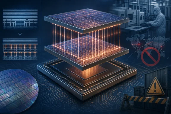 Huawei’s claim is about wiring, not a smaller transistor
Huawei introduced the Tau Scaling Law and LogicFolding at the IEEE International Symposium on Circuits and Systems in Shanghai on May 25. The company’s argument is that the important constraint in modern chips is increasingly the time required for signals to move through transistors and long metal interconnects, rather than transistor dimensions alone.
LogicFolding addresses that constraint by distributing portions of a circuit across two active silicon layers joined face-to-face using hybrid bonding. Put simply, a conventional planar layout must route signals sideways across a chip; Huawei wants to move selected logic blocks vertically, shortening high-priority paths and reducing the resistance-capacitance delay that slows electronic signals.
Huawei’s updated Tau paper says the first implementation was built at a fixed device node, rather than depending on a new lithography generation. It attributes up to a 55% increase in transistor density and up to a 41% improvement in performance-core power efficiency to the design. Those are significant figures if they hold up in shipping silicon, but they are Huawei’s measurements from its own work—not yet a broadly reproducible industry benchmark.
The most revealing detail is also the least glamorous one: the claimed gains come from topological reorganization. They do not establish that Huawei or Semiconductor Manufacturing International Corporation has solved the transistor, materials, patterning, and yield problems required for a production 1.4nm manufacturing process.
TSMC’s own A14 roadmap illustrates the divide. TSMC says its A14 process is on track for production in 2028 and describes it as a new manufacturing technology offering higher density, speed, and power efficiency than its 2nm generation. Huawei’s 2031 target is instead a density comparison across different combinations of process technology, circuit design, and three-dimensional integration. The two trajectories may produce chips with some comparable density figures, but they are not interchangeable measures of manufacturing capability.
LogicFolding builds on real 3D packaging work
The National Interest article presents folding as a response to constraints imposed by U.S. controls, which is broadly fair, but the engineering category itself is not new. Hybrid bonding, die stacking, chiplets, and vertical interconnects are already major parts of the global semiconductor industry’s strategy for sustaining performance improvements as shrinking transistors becomes more difficult and expensive.
TSMC, for example, has been commercializing its 3DFabric portfolio and says its 3nm system-on-integrated-chip stacking entered volume production in 2025. Other manufacturers have also used 3D packaging approaches to join compute, cache, and memory components more closely than conventional board-level or package-level connections allow.
Huawei’s potential contribution is narrower and more technically interesting than a slogan about bypassing Moore’s Law: it appears to be applying fine-pitch hybrid bonding and vertical partitioning inside the logic design itself, instead of reserving stacking mainly for memory or separately designed chiplets. Its paper describes reducing wire length, clock skew, and clock-tree complexity on a representative processing core.
That could be a useful advance for smartphone silicon, where power budgets and physical space are exceptionally tight. A handset chip has only a few watts to spare before sustained heat becomes a performance limiter, so a design that reduces data travel can improve responsiveness or lower power draw without increasing battery size.
But it also places Huawei in a harder engineering category than simply stacking a cache die on top of a CPU. Logic-on-logic stacking requires close attention to alignment, bonding defects, power delivery, test access, signal integrity, and heat removal. Those problems are why the industry has adopted 3D integration gradually, even where manufacturers have access to the most advanced lithography equipment.
Heat and yield will decide whether the density claim travels
The material unknown is whether Huawei can translate a carefully selected folded design into high-volume mobile processors with consistent performance. Huawei acknowledges in its technical paper that thermal management is central to further development. Putting active circuit layers close together reduces the distance signals travel, but it also makes it more difficult to remove the heat generated by those layers.
Hybrid bonding can offer electrical and interconnect-density advantages over older micro-bump techniques, and it can improve thermal contact at the bonding interface. That does not eliminate the package-level cooling problem. In a phone, the heat must still travel from the active silicon through the package, board, chassis, and ultimately into the surrounding air—or into the user’s hand.
Yield is the other constraint that deserves more attention than it receives in the promotional framing. A defect in either active tier, or in the bonding process itself, can make the final assembled device unusable. The simple multiplication often used to illustrate stacking penalties is directionally correct—two imperfect layers can lower the number of usable finished packages—but actual economics depend on whether Huawei uses wafer-to-wafer or die-to-wafer assembly, known-good-die testing, redundancy, repair strategies, die size, and defect density.
Huawei’s paper places unusually demanding requirements on alignment precision and bond yield. That is an admission that the architecture’s success rests as much on process control and packaging execution as it does on circuit ideas. A strong lab demonstration can establish that a design works. It cannot establish that enough of the design can be manufactured cheaply enough to supply a flagship phone line.
The National Interest also repeats estimates that SMIC’s advanced-node economics trail TSMC’s, but public data on SMIC’s current yields is limited. Assertions about a precise one-third yield ratio should therefore be treated as estimates rather than settled measurements. Neither SMIC nor Huawei publishes the kind of detailed defect, yield, and cost data that would let outsiders calculate the true production penalty of a folded Kirin processor.
The software bottleneck is as important as the package
Hardware alone will not make a 3D logic architecture practical. Engineers need electronic design automation tools that understand placement, routing, timing closure, thermal behavior, power integrity, testing, and manufacturability across multiple active layers. Existing EDA tools have years of optimization behind them for planar process flows and established advanced-packaging methods; a new logic-folding methodology must fit into an entire signoff and verification chain.
Huawei’s Tau paper calls for co-optimization across devices, circuits, chips, software, and systems. That is technically sound, but it also describes a vast dependency chain. A circuit architecture can be compelling while still being difficult to deploy because the design tools, IP libraries, package standards, test equipment, and manufacturing partners are not ready.
Reporting by Tom’s Hardware said Peking University had developed a prototype 3D EDA tool tailored to Huawei’s approach, based on reporting from the South China Morning Post. A prototype is a relevant start, especially in an area where China is trying to reduce dependence on U.S.-linked EDA suppliers. It is not evidence of a production-grade toolchain capable of turning out multiple complex SoCs on an annual smartphone cadence.
This is the place where export controls affect more than the lithography machine. U.S. Commerce Department rules restrict Chinese access to various advanced computing technologies and semiconductor-manufacturing capabilities, while the EDA market remains led by companies with deep libraries, specialized workflows, and longstanding foundry integration. Huawei can reduce one physical limitation through architecture without automatically removing the software and industrial dependencies around it.
The first Kirin launch will answer only part of the story
Huawei has officially said that Kirin chips launching in fall 2026 will be the first to adopt LogicFolding. It has not named those processors or the products that will contain them. Rumors identifying a Kirin 9050 and the Mate 90 series have circulated across mobile-focused outlets, but they remain rumors as of August 26, not a Huawei product announcement.
When the first device arrives, reviewers should look past peak CPU clocks and headline benchmark scores. The meaningful signs of success will be sustained performance under load, power consumption, skin temperature, modem and GPU behavior, die photography or package analysis where available, and evidence that the part can ship at volume rather than in a limited flagship run.
Huawei’s longer roadmap is more ambitious still. Its revised paper points to extending LogicFolding to an Ascend 990 AI accelerator around 2030. That would put the approach in a far more demanding environment: AI accelerators draw vastly more power than phone processors and are typically bottlenecked by memory capacity, memory bandwidth, and interconnect as much as by logic density.
For now, LogicFolding is a credible engineering direction rather than proof that Huawei has replaced leading-edge lithography. Its first consumer Kirin will show whether a vertically partitioned logic design can provide a meaningful mobile advantage at Huawei’s existing manufacturing base. The 2031 density target will remain a roadmap claim until Huawei demonstrates repeatable yields, thermals, design-tool maturity, and independently measured performance in products that ship beyond a single showcase device.