

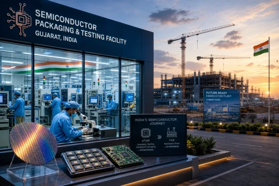
As reported by BISinfotech, Modi told the Red Fort audience on August 15 that chips have become indispensable to everything from phones and hospitals to transport systems, and said India expects another five to eight semiconductor plants to come online over the next seven to eight years. The speech ties chip capacity to Atmanirbhar Bharat, the government’s self-reliance program, and its wider Viksit Bharat development target.
For PC buyers, Windows hardware vendors and enterprise IT teams, the immediate effect is limited. India will not suddenly become a source of leading-edge processors for laptops, servers or AI accelerators. The more consequential development is that its semiconductor policy is moving beyond a narrow “build a fab” promise toward a subsidized domestic supply chain that could eventually support components used in PCs, networking gear, industrial systems and locally assembled devices.
Three operating plants are not three silicon fabs
The distinction matters because semiconductor plant can cover several very different operations. A wafer fabrication plant, or fab, turns silicon wafers into chips through thousands of processing steps and requires extraordinary capital investment, water, power, chemical handling and access to manufacturing technology. An outsourced semiconductor assembly and test facility—often called OSAT or ATMP—packages tested dies into the chips that device makers can mount on circuit boards.
India’s official Semicon 2.0 announcement says Micron, Kaynes and CG Semi have begun commercial production, with another company expected to begin in 2026. The government also says 12 manufacturing projects have been approved under the earlier program: one silicon fab, one silicon-carbide fab, an integrated gallium-nitride Micro LED facility, and nine packaging units.
That breakdown is far more informative than calling all three operational sites “fabrication factories.” Micron’s Gujarat facility, for example, is an assembly and test operation for memory products, not a DRAM wafer fab. Kaynes’ Sanand operation is also an OSAT facility. CG Semi, backed by CG Power, Renesas and Stars Microelectronics, operates in the same advanced packaging and testing segment.
Those activities are commercially important. Packaging determines how a chip connects to a motherboard, dissipates heat and, in advanced designs, combines several dies into one package. Modern AI and high-performance computing hardware increasingly depends on advanced packaging. Still, packaging capacity does not give a country the same control over leading-edge CPU, GPU, memory or logic-chip manufacturing as a high-volume silicon fab.
India has approved wafer-fab projects, including Tata Electronics’ planned Dholera facility in Gujarat, but approval, construction and commercial output are separate milestones. The government’s own figures make clear that India’s early production base is weighted toward back-end manufacturing rather than a mature domestic front-end wafer supply.
Semicon 2.0 shifts attention to the costly gaps around a fab
The major policy action predates Modi’s August 15 speech. On July 15, the Union Cabinet approved Semicon 2.0 with an outlay of ₹1,27,500 crore, or roughly ₹1.275 trillion. The Prime Minister’s Office described the program as a six-part effort spanning chip design, manufacturing, equipment and materials, advanced packaging, research and development, and workforce development.
That is a significant evolution from treating a fab announcement as the finish line. A fabrication plant cannot run competitively if it depends on imported specialty gases, photoresists, chemicals, ultrapure materials, spare parts, metrology systems and engineering talent for every stage of production. The Indian government is attempting to subsidize those surrounding capabilities as well.
The Indian Express reported that the new scheme places particular emphasis on suppliers of the gases and chemicals needed for chip production. Business Standard similarly reported that Semicon 2.0 expands support beyond fabrication into design, materials, equipment, advanced packaging, research and talent development.
For technology companies, that is the part of the plan worth watching. Chip projects often generate impressive investment totals long before they deliver predictable volume, qualified yields or supply-chain resilience. The success metric for India will not be the number of groundbreakings or even the number of facilities labeled “operational.” It will be whether local suppliers can meet stringent quality requirements repeatedly, whether facilities can recruit and retain process engineers, and whether the resulting chips find dependable customers.
The government says 105 start-ups and small or medium enterprises have gained access to industry-standard electronic design automation tools, while 24 semiconductor-design projects have received financial support. These are early-stage indicators, not proof of a self-sustaining design sector. But design capability is one area where India’s large engineering workforce could complement manufacturing and packaging investments, particularly in chips for telecommunications, power electronics, Internet of Things devices, cameras, smart meters and automotive systems.
The near-term output is more likely to affect mature chips than PC processors
Modi’s argument that “nothing” in the modern world works without semiconductors is broad but accurate in practical terms: Windows PCs, Wi-Fi gear, storage devices, monitors, smartphones, vehicles and medical equipment all rely on chips. The implication that domestic production will remove India’s technology dependence is much less immediate.
The approved Indian projects span a mixture of silicon fab, silicon carbide, display technology and packaging. Those categories point toward mature-node logic, memory packaging, power devices, automotive and industrial components, rather than the leading-edge x86 processors or GPUs that define premium PCs and data-center AI systems.
A modern laptop contains far more than its main processor. It uses power-management ICs, USB and Thunderbolt controllers, Wi-Fi and Bluetooth radios, display drivers, storage controllers, audio codecs, battery-management chips and embedded controllers. Many of those are made on established process nodes and could eventually be supported by a broader Indian manufacturing base. That could matter for locally assembled PCs and electronics, where imports, logistics disruption and currency exposure affect costs.
However, no policy document released with Semicon 2.0 identifies a domestic production timetable for leading-edge laptop CPUs, server processors or AI accelerators. Nor does it establish an equivalent of Taiwan’s mature foundry capacity, South Korea’s memory industry or the specialized machinery supply chain that supports them. For organizations planning Windows fleet purchases, there is no reason to expect this announcement to change availability or pricing for Intel, AMD, Qualcomm or Nvidia hardware in the short term.
The more immediate opportunity lies in packaging, component supply and equipment demand. As global vendors seek alternatives to concentrated manufacturing regions, India may become a more relevant location for qualifying back-end capacity and assembling electronics that use chips sourced elsewhere. That diversification can improve resilience without making India independent of foreign wafer suppliers.
The five-to-eight-plant target has no public project list yet
According to BISinfotech, Modi said India expects five to eight additional semiconductor plants to become operational within seven to eight years. The statement sets a direction, but it does not identify companies, locations, technology nodes, plant types, production volumes, incentive agreements or completion dates.
That missing detail is important. Five additional OSAT facilities would deepen India’s role in packaging and testing. Five additional wafer fabs, particularly at commercially meaningful scale, would be a vastly more difficult and expensive undertaking. The two outcomes carry very different implications for supply security, jobs, imports and domestic technology capability.
The official Semicon 2.0 material confirms 12 approved units and says one more company beyond Micron, Kaynes and CG Semi is expected to enter commercial production in 2026. It does not, at least in the public announcement, convert Modi’s five-to-eight figure into a project-by-project delivery schedule. Until the government publishes that roadmap, the speech should be read as a policy ambition rather than a contracted capacity forecast.
There is also a timing issue. A seven-to-eight-year horizon puts the target around 2033 or 2034. That is long in consumer technology terms. PC platforms may pass through several processor architectures, memory generations and packaging transitions before those promised plants reach volume production. The projects that succeed will need to match demand that does not yet exist, rather than simply duplicate today’s component mix.
What Windows and IT buyers should take from the announcement
India’s chip program is relevant to PC technology because hardware supply chains are no longer a background concern. Pandemic shortages, geopolitical restrictions and the rapid growth of AI infrastructure have shown how a disruption in one part of the semiconductor chain can delay entire classes of products. More packaging, materials and component capability in India could modestly reduce regional concentration over time.
But readers should separate a strategic industrial program from a near-term hardware change. Semicon 2.0 is real: it has Cabinet approval, a ₹1,27,500 crore budget and defined pillars that include equipment, materials and packaging. The government also confirms commercial production at three facilities. What has not been demonstrated is high-volume domestic production of the advanced chips that power mainstream Windows PCs, enterprise servers and AI workstations.
The practical milestone now is not another speech. It is the publication of project-level details for the next five to eight facilities, followed by evidence of reliable commercial output. Until then, India’s semiconductor push is best understood as a serious attempt to build a durable manufacturing base—one that has begun with packaging and support infrastructure, while the harder wafer-fab test remains ahead.
References
- PM Modi stresses semiconductor chips as key to technological - bisinfotech.com bisinfotech.com · 2026-08-17T06:20:33+00:00