
The report is plausible, but several of its most consequential details remain rumor rather than product specification. NVIDIA has publicly committed to Feynman in its 2028 data-center roadmap, including die stacking, custom HBM memory, and an optical NVLink generation. What it has not publicly said is that Feynman will use TSMC A16, TSMC-SoIC stacking, or a 50,000-wafer production ramp.
For enterprises budgeting AI infrastructure, the practical signal is less about a “1.6nm GPU” arriving in two years than it is about where NVIDIA’s bottleneck is moving. Feynman is shaping up as a rack-scale platform whose performance, deployment density, cooling requirements, optical interconnects, and packaging supply could matter as much as the GPU core itself.
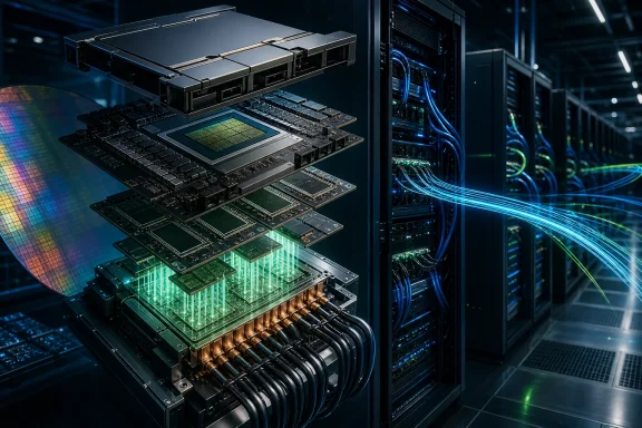 A16 is an N2-family extension, not a simple node-number leap
Calling Feynman a “1.6nm” product is useful shorthand, but it can mislead. Modern process-node labels are brand names rather than literal measurements of transistor features. TSMC calls A16 a 1.6nm-class technology, but the number should not be read as a physical transistor-gate length.
More importantly, A16 is not a clean break from TSMC’s 2nm work. In its 2026 annual-meeting materials, TSMC described both N2P and A16 as extensions of its N2 family. N2 entered high-volume manufacturing in the fourth quarter of 2025, while TSMC says N2P and A16 are scheduled for volume production in the second half of 2026.
The distinguishing feature is TSMC’s Super Power Rail, its implementation of backside power delivery. Conventional chips route power and data signals through metal layers above the transistors. Backside power delivery moves the power rails to the other side of the wafer, freeing front-side routing resources for signals and reducing voltage drop.
TSMC positions A16 specifically for high-performance computing chips with difficult signal-routing and power-delivery requirements. It claims an 8% to 10% speed improvement at the same voltage, or 15% to 20% lower power at the same speed, compared with N2P, along with up to a 10% density increase. Those are foundry projections, not Feynman performance estimates, and they cannot be translated directly into GPU benchmark gains.
The timing also makes the rumored choice less dramatic than the headline implies. If A16 enters volume production in late 2026 and Feynman does not reach volume production until late 2028, NVIDIA would be adopting a process with roughly two years of manufacturing maturation behind it. That is still an aggressive node choice for an AI accelerator, but it is not the same as shipping at A16’s launch.
NVIDIA has confirmed Feynman’s direction, not its foundry recipe
NVIDIA’s March 2026 GTC roadmap did establish that Feynman is a real successor platform, not an invented codename. Jensen Huang described it as a 2028 generation with a new GPU, the LP40 language-processing unit, the Rosa CPU, BlueField-5, ConnectX-10 networking, and scale-up systems using both copper and co-packaged optics.
NVIDIA’s own roadmap also lists die stacking, custom HBM, and NVLink 8 with co-packaged optics for Feynman. Those are consequential changes. A stacked design would allow NVIDIA to pursue more compute density without relying only on a larger monolithic die, while custom HBM suggests the company expects memory capacity, bandwidth, and power delivery to become still tighter constraints.
But the public NVIDIA roadmap does not name TSMC A16, SoIC, AP7, AP8, or a specific HBM generation. It also does not identify the GPU die count, the package dimensions, power envelope, memory capacity, or whether any part of the Feynman family will appear in workstation or GeForce products.
That gap matters because the TweakTown report presents TSMC’s System on Integrated Chips, or SoIC, as the mechanism for Feynman’s 3D chiplets. NVIDIA has confirmed die stacking, but it has not confirmed SoIC. TSMC, for its part, says it is developing SoIC alongside CoWoS, InFO, and its COUPE photonics technology; it has not publicly attached any of them to Feynman.
SoIC is a plausible fit for vertical integration, but plausible is not confirmed. Administrators and buyers should avoid treating a packaging rumor as a finalized NVIDIA architecture.
The A16 report has support, but no official customer confirmation
The basic A16-Feynman claim did not begin with this week’s DigiTimes report. In September 2025, Tom’s Hardware reported that China’s Commercial Times had identified NVIDIA as TSMC A16’s first customer and said Feynman could skip standard N2. In March 2026, TrendForce, citing Taiwan’s TechNews, similarly reported that Feynman was expected to use A16.
Those reports make the underlying direction more credible than a single fresh leak. They still do not amount to a formal customer announcement. Neither NVIDIA nor TSMC has publicly named a first A16 customer, and neither has published a Feynman tape-out, wafer-order, or production schedule.
The second-half-of-2028 timing remains particularly thin. TweakTown’s DigiTimes-based account is the source for that specific window, and no official NVIDIA release has narrowed Feynman’s public 2028 target to a half-year. NVIDIA’s annual cadence has been ambitious, but roadmap years are not shipping commitments for every product and configuration.
The report’s claim that TSMC is accelerating AP7 and AP8 construction, with an aim of 50,000 wafers by the end of 2027, should be treated the same way. TSMC’s public materials confirm continued investment in leading-edge and advanced-packaging capacity, but they do not confirm those facility names, that output figure, or an allocation to NVIDIA.
Packaging and optics may be the real deployment constraint
If Feynman reaches production with stacked dies, custom HBM, and co-packaged optics, the limiting factor may not be A16 wafer capacity alone. NVIDIA’s largest AI systems already depend on advanced packaging, high-bandwidth memory, network silicon, optical components, liquid cooling, and full-rack power delivery arriving together.
NVIDIA’s current Vera Rubin documentation illustrates the direction. The company describes a Rubin NVL72 system with 72 GPUs and 36 Vera CPUs tied together through an NVLink copper spine, while the 2027 Rubin Ultra roadmap expands the scale-up domain to 576 GPUs. For the next phase, NVIDIA says the Kyber rack architecture can scale to an NVL1152 system through direct optical interconnects and will provide the foundation for Feynman-era extreme scale-up computing.
That makes the Feynman story a data-center design story, not simply a GPU fabrication story. Co-packaged optics could reduce the electrical and power penalties of moving data across very large scale-up domains, but it adds a new class of component integration and serviceability concerns. A failed optical component in a conventional pluggable-optics design is a familiar field-replaceable event; putting optical engines closer to switching silicon changes the economics and operational model.
NVIDIA has publicly committed to optical scale-up for Feynman, but it has not supplied failure-rate, repair, spare-part, or field-service information for the platform. Those details will matter far more to AI-factory operators than whether a roadmap graphic carries an A16 label.
No consumer-GPU implication has been established
Nothing in the reporting establishes that Feynman will be an RTX or consumer desktop GPU architecture. NVIDIA’s confirmed Feynman material concerns its data-center roadmap, including AI accelerators, CPUs, LPUs, networking, and rack-scale systems. The submitted report likewise discusses AI and data-center products.
Windows PC users should therefore resist reading the A16 rumor as an early indication of a GeForce release date, RTX 6000-series specifications, or a reason to postpone a workstation upgrade. There is no public Feynman client-GPU roadmap, no confirmed gaming SKU, and no statement that the A16 node would be used across NVIDIA’s consumer portfolio.
For data-center planners, the more concrete takeaway is that NVIDIA is publicly preparing a 2028 platform built around stacked compute, custom memory, and optical scale-up, while multiple reports point to TSMC A16 as the likely process choice. The node is credible; the exact production window, SoIC implementation, capacity reservation, and final system configuration are still unverified.
