
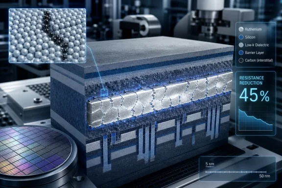
The practical result, reported by The Chosun Ilbo and independently described by Edaily, is a roughly 45% reduction in line resistance versus comparable ruthenium wiring without the carbon-based promoter. For PC and server buyers, this does not mean a faster Samsung SSD, CPU, or AI accelerator is about to ship. It is a materials result aimed at a bottleneck that grows more severe as chipmakers shrink wiring and stack more circuitry vertically.
Samsung and the Gwangju Institute of Science and Technology, or GIST, developed the work with a research group dominated by Samsung authors. Edaily also reports participation by researchers at MIT, an affiliation omitted in the original Chosun Ilbo report. The published paper lists 13 authors; 11 are reported to be from Samsung’s SAIT research organization.
 Carbon is being used to control the metal, not to replace it
The advance concerns ruthenium, or Ru, a metal under active consideration for ultra-small interconnects. Chips contain many layers of wiring above the transistors. Those wires are not passive plumbing: their resistance affects switching delay, voltage drop, heat, and the energy required to move data around a processor, GPU, memory device, or accelerator.
Copper has long been the standard interconnect metal, but it becomes harder to use efficiently as lines narrow. At extreme dimensions, barriers and liners needed to keep copper from diffusing into surrounding materials consume an increasing share of the available cross-section. Surface scattering and grain boundaries also punish conductivity. Ruthenium is attractive partly because it can potentially reduce or eliminate some of that overhead, but ruthenium itself still faces a familiar nanoscale problem: electrons are disrupted as they cross poorly arranged crystalline grains.
Samsung’s team did not claim to have found a radically lower-resistivity metal. Instead, it used a trace carbon promoter during recrystallization to change how ruthenium grains form. The carbon creates temporary free volume at grain boundaries, according to the Science paper’s abstract, allowing atoms to migrate and the metal grains to reorient as the film recrystallizes.
The stated outcome is a ruthenium film in which more than 99% of the crystals share a preferred out-of-plane orientation, while grain boundaries predominantly take lower-energy forms. That degree of texture matters because a nanoscale wire with fewer disruptive boundaries offers electrons a less obstructed path. In the line test highlighted by Edaily, the approach reduced resistance by about 45%.
This is more specific than the broad “carbon improves wiring” framing suggests. Carbon is a transient processing aid in the reported mechanism, not a permanent bulk ingredient intended to turn the wire into a carbon-based conductor. The engineering target is the microstructure of the final ruthenium film.
The paper date exposes a small but telling discrepancy
The initial report said the research was published in Science on August 13, local time. The paper record for DOI 10.1126/science.ady9591 identifies a publication date of August 14, 2026. That one-day mismatch may reflect an online-release timing or a time-zone conversion, but neither Samsung nor the reports reviewed here publicly explains it.
It is a minor discrepancy, yet it illustrates why the marketing language deserves separation from the experimental result. The peer-reviewed paper establishes the material-science finding: promoter-driven recrystallization produced highly textured ruthenium without relying on lattice-matched epitaxial growth. It does not, by itself, establish that Samsung has solved interconnect scaling in a production logic process, let alone that the process is ready for a named fabrication node.
Likewise, “world first” is not a measurement. Neither The Chosun Ilbo nor Edaily identifies the earlier approaches being surpassed, defines the scope of the comparison, or supplies a third-party priority assessment. The defensible claim is narrower and still significant: Samsung-led researchers have demonstrated a carbon-promoted route to highly oriented ruthenium films and a large resistance improvement in the tested nanoscale wiring structure.
The research also has a longer trail than the announcement implies. Samsung-linked patent filings published before this paper describe ruthenium thin films with strongly controlled grain orientation and low grain-boundary misorientation. Samsung researchers presented grain-orientation engineering of atomic-layer-deposited ruthenium interconnect technology at the IEEE International Electron Devices Meeting in December 2025. In other words, this is a result emerging from a continuing interconnect program, not a sudden one-off laboratory discovery.
Why the 45% number should not be read as a 45% faster chip
Line resistance is only one contributor to a chip’s speed and power profile. A processor’s delivered performance also depends on transistor characteristics, cache and memory architecture, clock targets, routing choices, packaging, power delivery, software, and thermal limits. Even within a chip, only the wiring layers and dimensions that can use this ruthenium process would benefit.
A 45% reduction in a measured wire’s resistance therefore cannot be translated honestly into a 45% gain in CPU performance, GPU throughput, or AI inference efficiency. Samsung did not announce a commercial process node, customer design win, qualification milestone, reliability target, or production schedule. No current Windows PC, data-center GPU, or Samsung consumer product is known to use this process.
The more immediate consequence is for the design budget available to future chips. Lower resistance can let engineers trade the gain among lower power, lower delay, more routing flexibility, or some combination of those outcomes. That tradeoff becomes more valuable in AI and high-performance computing silicon, where data movement across large dies and through stacked structures can consume substantial energy.
Edaily reports that the team tested applicability to wiring around 2 nanometers wide and to complex three-dimensional structures. If the result survives integration, that is arguably the most consequential part of the work. Future logic and memory designs increasingly rely on vertical structures, where deposition and material uniformity become harder than they are on flat surfaces.
Integration, reliability, and cost remain the real tests
A promising blanket film is far from a qualified interconnect module. Production deployment would require the ruthenium deposition, carbon-promoter step, anneal, patterning, etch, dielectric interaction, barrier strategy, and cleaning sequence to work together across full wafers at high yield.
The unanswered reliability questions are substantial. Chipmakers will need to establish whether the reoriented structure remains stable through later high-temperature manufacturing steps; whether it withstands electromigration under long-term current stress; whether contact resistance offsets some of the line-resistance gains; and whether the method works consistently in the dense, high-aspect-ratio features used by real advanced designs.
There is also a manufacturing economics question. Ruthenium is not copper, and a process can be electrically attractive without being commercially viable at the scale of a leading-edge fab. The study’s value lies in showing that crystal orientation can be engineered with a trace promoter on amorphous dielectric substrates, where conventional epitaxial control is unavailable. Whether that extra control can be delivered with acceptable cost, throughput, defectivity, and yield is the bridge Samsung still has to cross.
Samsung’s own prior work on area-selective ruthenium deposition underlines the point. Modern interconnect manufacturing is not merely about making a conductive film; it is about placing the right material exactly where it belongs while avoiding growth, damage, or contamination elsewhere. The current result improves one hard part of that broader process stack.
This is a credible research milestone, not a product announcement
The strongest reading of Samsung’s announcement is that it advances a credible candidate for post-copper or copper-complementary nanoscale wiring. The paper’s mechanism is concrete, the measured resistance result is meaningful, and the work addresses a constraint that will directly shape future processors, memory, and AI accelerators.
But readers should resist treating this as evidence that a 2 nm Samsung process is now in mass production or that a near-term PC upgrade will inherit a 45% performance boost. Samsung has disclosed no production node, no product, and no timetable. The next meaningful milestone will be a demonstration that the carbon-promoted ruthenium structure can survive a complete interconnect integration flow with published reliability and yield data.