
Chosunbiz, citing Taiwanese media including the Liberty Times, reported that TSMC has completed development and validation of the 1.6nm-class A16 process and is preparing volume manufacturing for AI and high-performance computing chips. That timetable matches TSMC’s own public technical disclosure, which said A16 mass production was slated for Q4 2026, as well as the company’s June shareholder-meeting materials, which broadly placed A16 volume production in the second half of the year.
The distinction is worth making for PC and enterprise buyers watching the AI-chip supply chain. A16 is not shipping silicon today, and TSMC has not identified launch customers, wafer volumes, product names, or the factories that will handle its initial ramp. What has been corroborated is that the process has moved through qualification and is planned for the transition from development to manufacturing late this year.
 A16 is TSMC’s backside-power bet for dense AI designs
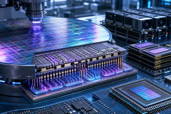
A16 combines TSMC’s nanosheet transistor technology with a backside power-delivery design called Super Power Rail, or SPR. Conventional logic chips place both signal wiring and power distribution on the front side of the wafer, forcing designers to allocate increasingly scarce routing space between the two jobs. A16 moves the power network to the backside and uses direct backside contacts to feed transistor source and drain regions.
The immediate engineering purpose is to free front-side metal layers for data signals. That matters most in chips where vast numbers of compute blocks, cache structures, high-speed interfaces, and memory connections compete for routing resources. AI accelerators and large server processors are obvious candidates; they have become harder to scale simply by shrinking transistors because delivering stable power and connecting all those blocks is now a central design constraint.
TSMC says SPR reduces voltage drop in the power network while preserving the gate density, layout footprint, and device-width flexibility available with traditional front-side power delivery. The company’s A16 technical material also says the process retains its NanoFlex design-technology co-optimization approach, allowing chip teams to choose different nanosheet cell configurations depending on whether a block needs maximum speed or better density and efficiency.
This is why TSMC has consistently positioned A16 for particular HPC designs rather than as a universal replacement for its 2nm family. A client chip with relatively ordinary routing demands may see less reason to absorb the cost and design complexity of a backside-power platform. A large GPU, AI accelerator, custom cloud ASIC, or high-end server CPU with dense power grids has a clearer reason to use it.
The “1.6nm” description should also be read as a process-generation label, not a literal measure of a transistor feature. Modern node names no longer correspond to one physical dimension such as gate length. The practical comparison is the one TSMC itself provides: A16 is an extension beyond N2P, the performance-enhanced version of its 2nm N2 process, rather than an entirely unrelated manufacturing family.
The Q4 date is a manufacturing milestone, not a product-release calendar
TSMC’s VLSI Symposium abstract stated that it had developed and qualified the A16 platform and expected mass production in Q4 2026. That independently corroborates the central claim in the Chosunbiz report. It also suggests that the report’s reference to completed validation is not an unverified last-minute development, but a description of a qualification stage TSMC had already discussed publicly in June.
The company’s 2025 annual report and its 2026 annual meeting minutes had used less precise language, putting N2P and A16 volume production in the second half of 2026. The technical-paper Q4 target narrows that window, though it remains a target. Semiconductor production ramps can still be affected by yield, tool availability, customer qualification, packaging capacity, and demand forecasts between August and the end of the year.
For readers expecting an immediate effect on Windows PCs, that means patience. Even after TSMC begins volume manufacturing, A16 wafers must be processed, packaged, tested, integrated into finished processors or accelerators, validated by system makers, and shipped through server or device channels. The first commercial products using the process are more likely to appear in specialized AI and datacenter hardware than in mainstream consumer PCs.
TSMC has not named an A16 customer or announced a Windows-PC processor built on the node. Any claim that a particular Nvidia, AMD, Apple, Qualcomm, Microsoft, or custom-cloud chip will be first would therefore be speculation. The credible conclusion is narrower: A16 expands the manufacturing options available to chip designers whose products are constrained by power delivery and interconnect density.
TSMC’s published targets place A16 at an 8% to 10% speed improvement at the same power versus N2P, or a 15% to 20% power reduction at the same speed. It also projects up to 10% more chip density. Those are process-level targets, not promises for every finished processor. A customer’s real result depends on architecture, libraries, SRAM choices, interconnects, voltage targets, packaging, cooling limits, and the portion of the design that can benefit from extra front-side routing capacity.
Backside power addresses a bottleneck that transistor shrinks alone cannot fix
For decades, chip scaling largely rewarded designers with smaller, faster, and more power-efficient transistors. Leading-edge designs now face a more complicated problem: even if transistor devices improve, the surrounding wiring and power network can limit the usable gain. As switches become denser and currents rise, power must travel through a crowded stack of metal layers without causing excessive voltage loss, noise, heat, or signal-routing compromises.
Backside power delivery attacks that system-level constraint. By relocating power distribution, designers get more front-side wiring capacity for signals, while power can take a shorter or more direct route to the transistors that consume it. In theory, that can improve performance, reduce energy use, and make an extremely large die easier to route.
The approach is technically demanding. It adds process steps and requires highly precise backside alignment and contact formation after substantial front-side work has already been completed. TSMC’s claim that A16 preserves N2P’s gate-density and layout flexibility is therefore significant: backside power is valuable only if it does not create design restrictions that erase its routing advantage.
Intel is also pursuing backside power delivery through its PowerVia technology, making this one of the important manufacturing contests in advanced logic. The comparison should not be reduced to node-name marketing. The relevant question for customers is whether each foundry can combine transistor performance, power delivery, usable libraries, yield, packaging, capacity, and predictable ramp schedules into products that can be designed and shipped at scale.
TSMC’s A16 positioning is more selective than a claim that every chip needs backside power immediately. The company is directing it toward designs with complex signal routes and dense power-delivery networks, while N2P remains the broader enhancement path in its 2nm family. That split gives customers a choice: use N2P where its design rules and economics are sufficient, or adopt A16 when routing and power constraints justify the more advanced platform.
Packaging capacity may decide how much A16 matters in practice
The Chosunbiz report also links A16 to continued investment in advanced packaging, particularly the Chip on Wafer on Substrate, or CoWoS, family used to connect large logic dies with high-bandwidth memory and other components. The connection is real even though A16 and CoWoS solve different problems. A16 improves the logic die; advanced packaging determines how that die is combined with memory and neighboring chiplets into a usable AI system.
TSMC’s board approved roughly $29.4 billion in capital expenditures on August 11 for advanced process, advanced packaging, and other capacity. The board authorization is an official corporate action, but it does not break out how much is earmarked for A16 versus N2P, A14, CoWoS, or other investments. It should not be read as an A16-specific spending figure.
The article’s claim that some advanced-packaging volumes are moving to Intel’s Malaysia operations is more difficult to establish from public primary records. Chosunbiz attributes that account to industry reporting, but neither TSMC nor Intel has publicly identified an A16-related outsourcing arrangement. It is therefore too early to treat any such handoff as a confirmed feature of TSMC’s production plan.
What is clear is that an AI accelerator cannot become a deployable server product merely because its logic die is ready. High-bandwidth memory availability, CoWoS or equivalent packaging slots, substrates, validation capacity, and server-platform integration all influence actual shipments. The chip industry’s recent AI bottlenecks have repeatedly moved beyond the transistor fab to those downstream stages.
TSMC’s A16 milestone is therefore a meaningful manufacturing checkpoint, not a signal that a new generation of AI PCs or servers is about to appear. The concrete event to watch is whether TSMC confirms a successful Q4 2026 volume ramp and whether customers subsequently disclose products built on the process. Until then, A16 is a qualified, scheduled technology platform whose strongest promise is more routing and power-delivery headroom for the largest and most demanding AI and HPC chips.
