
 Overview: The “Inert Substrate” Assumption Is Under Pressure
For decades, the standard mental model of a thin-film electronic device has been straightforward. The thin film is the functional layer: it conducts, switches, changes phase, emits light, senses a signal, or stores information. The substrate is the supporting platform, selected for properties such as lattice matching, thermal conductivity, electrical insulation, mechanical strength, and manufacturability.
That model remains useful, but the new work argues that it is incomplete.
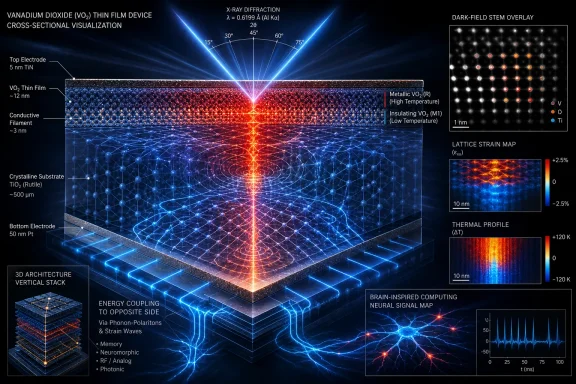
Researchers led by UC San Diego physicist Alex Frañó found that when a voltage drives switching activity in a vanadium dioxide thin film, the substrate also changes. Rather than serving only as a rigid passive base, it appears to participate in a reciprocal interaction with the active film—a process the team characterizes as coupling and describes metaphorically as a “dance.” UC San Diego
The immediate importance is not that every substrate in every electronic product is suddenly an active computing component. It is that the film–substrate interface may be a much more consequential part of device behavior than designers have typically treated it to be. In materials where electrical activity, strain, heat, atomic arrangement, and phase changes are tightly linked, that distinction could become central.
For Windows PC users and hardware enthusiasts, this is a reminder that tomorrow’s compute efficiency gains may not come solely from smaller transistors or faster memory interfaces. They may come from materials that make a single physical device perform functions usually spread across transistors, capacitors, memory cells, and interconnects.
Why Vanadium Dioxide Matters for Brain-Inspired Computing
The device at the center of the study uses vanadium dioxide, commonly written as VO₂. It is a quantum material known for an abrupt transition between electrically insulating and more conductive states. Under an electrical stimulus, VO₂ devices can exhibit sharp threshold switching and transient conductive behavior—characteristics that researchers have investigated for unconventional memory, switching, and neuromorphic systems. NIST’s overview of quantum materials for neuromorphic computing
That behavior is especially attractive to teams pursuing neuromorphic computing. Conventional computers generally separate processing and memory, moving information repeatedly between logic units and storage. The approach is exceptionally flexible, but moving data can consume substantial energy and impose latency.
Neuromorphic designs instead seek to imitate selected features of biological neural networks:
- Spiking behavior, where activity occurs as discrete events rather than as a continuously clocked stream.
- Threshold responses, where a device reacts only after an input crosses a defined level.
- Local memory and computation, reducing the need to shuttle every datum to a distant processor.
- Rich physical dynamics, where properties such as resistance, heat, magnetization, or phase state become part of the computation.
Quantum materials are compelling in this context because their collective electronic and structural behavior can be highly nonlinear. A relatively small electrical input can produce a disproportionately large change in state, potentially providing neuron-like or synapse-like functions directly in hardware. NIST
The UC San Diego team’s VO₂ thin films form an electrically conductive filament when a voltage is applied. The resulting electrical spiking is analogous, in a limited device-physics sense, to the spikes that neurons use to communicate. The analogy should not be overstated: a thin-film switch is not a biological neuron, nor does a single switching event constitute intelligence. But it can supply a primitive physical behavior that software and conventional CMOS circuits must otherwise synthesize with many components. UC San Diego
Filaments Are More Than a Curiosity
Conductive filaments are vital to the discussion because they concentrate current and energy into a narrow region. In threshold-switching materials, that localized activity can set off feedback between electrical conductivity and temperature, producing rapid changes in the device state.
Research from the National Institute of Standards and Technology has highlighted how current constriction can emerge in threshold-switching devices, particularly in materials whose electrical properties vary sharply with temperature. Such localized current distributions are important because they complicate the assumption that a device behaves uniformly across its full area. NIST’s work on spontaneous current constriction
The new UC San Diego result extends that concern beyond the active VO₂ film itself. If the film’s localized switching drives detectable changes in the substrate, then engineers may need to consider a larger physical system: electrodes, film, interface, substrate, mounting environment, and the pathways through which strain or thermal energy move.
The Unexpected Result: The Substrate Moves Too
The research team began by applying a new imaging approach to working vanadium dioxide thin-film devices. Its key observation was that the substrate changed alongside the film under electrical stimulation, indicating reciprocal behavior rather than one-way influence. UC San Diego
This matters because the dimensional imbalance is severe. The report describes the active thin film as roughly 100 nanometers thick, while the substrate can be about 10,000 times thicker. Conventional intuition says that such a thin active layer should have little ability to influence the larger foundation substantially.
Yet the team observed the opposite: the thin film could push and pull on the substrate, while the substrate also acted back on the film. Frañó compared the effect to a tree on a mountaintop moving the entire mountain beneath it. UC San Diego
The metaphor is useful because it conveys the surprise without pretending the substrate literally moves like a macroscopic object. The important mechanism is a coupled response in the material system. Depending on the device architecture and the measurement conditions, that could involve strain, lattice distortion, thermal transfer, altered crystal structure, or related changes in the local energy landscape.
A Revision to Device Design Thinking
The practical consequence is not “discard all substrates.” It is more specific and more demanding: treat the substrate as an active design variable when studying strongly responsive thin films.
That may require engineers to rethink several conventional choices:
- Substrate material selection
A substrate may no longer be chosen only for mechanical support, insulation, or compatibility with deposition methods. Its structural and thermal response could influence switching behavior. - Substrate thickness
The UC San Diego team reports changing substrate thickness as part of its validation work. If thickness affects coupling, it becomes an electrical and functional parameter rather than merely a packaging or handling choice. UC San Diego - Interface engineering
The boundary between a thin film and its substrate may be as important as the film’s composition. Defects, strain, adhesion, lattice mismatch, and fabrication-induced disorder could all affect the interaction. - Circuit modeling
Compact models that assume a fixed, passive foundation may miss behavior relevant to oscillation stability, repeatability, thermal drift, and device-to-device variation. - Three-dimensional integration
A substrate that can transmit useful coupling may become a medium for connecting functional layers on opposite sides rather than simply separating them.
That last point is particularly provocative. The UC San Diego team suggests that materials on either side of a substrate could potentially be coupled through it, offering a route toward more interconnected, three-dimensional hardware. UC San Diego
Dark-Field X-Ray Microscopy Was the Enabling Tool
Scientific breakthroughs are often as much about measurement as they are about materials. In this case, the team’s new perspective came from dark-field X-ray microscopy, developed in the project by graduate researcher Elliot Kisiel.
Dark-field X-ray microscopy is designed to image selected diffraction features and can reveal structural variations—including lattice orientation and strain—in ways that conventional full-field imaging may not capture as directly. Work at Argonne National Laboratory’s Advanced Photon Source has shown that dark-field X-ray microscopy can produce three-dimensional views of material regions that reveal lattice orientations, strains, and mesoscale structures. Argonne’s Advanced Photon Source
Kisiel’s stated goal was to bridge strengths associated with electron microscopy and X-ray diffraction. In the UC San Diego account, the method allowed the researchers to view an entire device in one image while retaining high-fidelity information about the surrounding material. That last capability proved decisive because it allowed the researchers to look beyond the expected action in the thin film and inspect the substrate itself. UC San Diego
Why Looking Around the Device Changed the Story
There is an instructive lesson here for semiconductor and materials research. Measurements are frequently optimized to find a known effect as clearly as possible: the switching channel, the active layer, the transistor gate, the memory cell, or the optical region of interest.
But a measurement focused too tightly can make the environment disappear from the scientific model.
The team initially turned attention toward the substrate for pragmatic reasons. X-ray lenses can absorb much of the radiation that passes through them, so the researchers sought a target that delivered more signal during preliminary testing. That detour revealed that the surrounding “inactive” material was responding. UC San Diego
It is a classic example of instrumentation expanding the boundaries of the question. Instead of asking only, What is the thin film doing?, the experiment made it possible to ask, What is the entire device stack doing while the thin film switches?
That is likely to be the more valuable question for next-generation computing materials.
Reproducibility Gives the Result Weight
The strongest part of the report is not merely that the team saw a surprising signal. It is that the researchers reportedly spent four years testing whether the observation would survive attempts to break it.
According to UC San Diego, the group reproduced the effect using the original approach, then varied characteristics including substrate thickness and substrate material. It also examined the behavior with different instrumentation at Argonne National Laboratory and Brookhaven National Laboratory. UC San Diego
That matters because coupled structural and electrical phenomena are exactly where false positives can hide. A surprising measurement might otherwise be explained by instrumental artifacts, sample damage, localized heating, mechanical mounting effects, inconsistent fabrication, or an unusual feature in one particular device.
The report’s emphasis on repeated experiments, altered sample conditions, and multiple facilities does not eliminate every future question. No single paper can map every possible material, geometry, temperature range, operating frequency, and fabrication pathway. But it does provide a more credible foundation than a one-off observation.
The use of complementary high-end facilities is also significant. Argonne’s synchrotron capabilities are designed for high-brightness X-ray studies, while Brookhaven operates ultrafast electron microscopy capabilities intended to observe materials and devices in operation. UC San Diego
What It Could Mean for Three-Dimensional Computing Hardware
For much of the semiconductor industry, moving into the third dimension has become necessary rather than optional. Modern systems already use methods such as stacked memory, advanced packaging, chiplets, through-silicon vias, and vertical transistor structures to increase density and shorten connections.
However, these approaches still confront difficult trade-offs:
- Heat removal becomes more challenging as layers are stacked.
- Fabrication complexity rises with alignment, bonding, and yield requirements.
- Interconnect delays can remain a limiting factor even when devices are densely packed.
- Power delivery and signal integrity become harder to manage in tightly integrated structures.
- Defects and stress can propagate across layers or interfaces.
The UC San Diego finding introduces a different possibility: a substrate might function as a coupling medium between devices on opposite sides. That is not equivalent to a finished vertical interconnect technology, and it does not automatically replace metal wiring. But it suggests that physical interactions through a substrate—possibly structural, thermal, or collective—could become computationally useful rather than merely undesirable. UC San Diego
The Appeal for Neuromorphic Architectures
Neuromorphic systems do not necessarily need every connection to behave like a conventional binary wire. In biological neural networks, timing, oscillation, local adaptation, and collective dynamics can be as important as static digital states.
That is why coupling is attractive. If a substrate can help mediate interactions between elements without each connection requiring a conventional transistor-and-wire pathway, it could enable new architectures with a different balance of density, energy use, and computational behavior.
Q-MEEN-C, the Department of Energy-supported research center associated with the work, frames its mission around developing quantum-material foundations for energy-efficient, fault-tolerant brain-inspired computing. Its research plan explicitly includes exploring collective and frequency-selective mesoscale coupling as a route to novel connectivity. DOE’s Q-MEEN-C overview
The substrate discovery therefore fits into a broader effort to identify ways in which materials themselves can supply connectivity and dynamics. It is less about building a faster version of a conventional CPU core and more about discovering what hardware becomes possible when the material stack is treated as an active computational system.
The Risks: A New Degree of Freedom Can Become a New Failure Mode
The study’s upside is substantial, but so are the engineering complications. The word coupling sounds positive when it refers to useful device communication. In manufacturing and reliability engineering, however, unintended coupling is often a source of noise, drift, instability, and poor yield.
A substrate that responds to thin-film switching could create new opportunities. It could also make precise control more difficult.
Device Variability May Become Harder to Manage
Thin-film and phase-transition devices already face challenges involving variation across a wafer and between nominally identical devices. If substrate properties alter threshold behavior or switching dynamics, then variations in substrate composition, thickness, surface preparation, crystal orientation, or stress could influence performance.
This does not make the devices impractical. It does mean process control must likely become more sophisticated. The right substrate could enhance a desired effect, while the wrong variation could blur it.
Thermal and Mechanical Crosstalk Need Close Study
VO₂ switching and conductive filament formation can involve strong local energy concentration. The discovery that the substrate participates raises critical questions about the separation of mechanical, thermal, and structural effects.
For example:
- Does substrate coupling improve repeatability or worsen it?
- Does the effect persist at high switching rates?
- Can adjacent devices affect one another unintentionally?
- Does the response change as a device ages?
- How do encapsulation and packaging materials modify the coupling?
- Can designers distinguish productive coupling from parasitic crosstalk?
These are not objections to the research. They are the next engineering agenda.
The broader literature on VO₂ devices reinforces why such detail matters. Operando studies have shown that conductive filaments and volatile resistive switching in VO₂ are central to its potential for neuromorphic electronics, but the microscopic mechanisms and device states involved can be complex. A peer-reviewed operando study of conductive filaments in Mott VO₂
Better Performance Is Not Guaranteed
It would be premature to translate this result directly into claims about commercial energy savings, processor speed, consumer PC upgrades, or AI accelerators. The research establishes a new materials interaction and a possible design direction; it does not announce a shipping processor or demonstrate a completed 3D neuromorphic chip.
The route from a high-resolution materials observation to a manufacturable computing platform is long. It must pass through reproducible fabrication, integration with control circuitry, endurance testing, thermal characterization, error behavior, wafer-scale uniformity, software mapping, and cost analysis.
Still, early-stage materials findings matter precisely because they shape what those later stages attempt to build.
A Different Definition of “Active” Hardware
The larger significance of this work is philosophical as much as technical. Modern computing design often divides a system into active and passive components: logic versus packaging, transistors versus supports, computation versus structure.
The UC San Diego team’s result weakens that boundary.
If a substrate can exchange energy with a thin film under operating conditions, then the substrate is not merely a backdrop. It may be part of the device’s functional behavior. That shifts the design question from How can engineers isolate the active material from everything else? to How can they deliberately control the whole interacting system?
That perspective is already common in some corners of advanced materials research, where interfaces, strain, lattice behavior, and collective effects can determine a device’s useful properties. The new study makes the point unusually tangible by showing a massive substrate responding to a nanoscale switching layer. UC San Diego
For the future of energy-efficient AI hardware, that may prove more important than the headline metaphor. The “dance” is not simply a surprising visual. It is evidence that a computing device can be a network of interacting materials long before it becomes a network of transistors.
Conclusion: The Mountain Is Part of the Machine
The UC San Diego research does not overturn conventional semiconductor design overnight. Thin-film substrates will still be chosen for stability, compatibility, thermal behavior, cost, and manufacturability. Conventional CMOS will remain essential to Windows PCs, servers, GPUs, and the vast majority of practical computing systems for the foreseeable future.
But the discovery adds a consequential new rule for researchers exploring quantum materials and neuromorphic devices: the substrate cannot automatically be treated as inert.
In vanadium dioxide thin-film devices, the active layer and its foundation appear to act on one another under voltage. That interaction could become a challenge to control, a new source of device behavior to model, or a pathway to denser and more biologically inspired computing architectures. Most likely, it will be all three.
The next advances will depend on turning this coupled behavior from an unexpected observation into a programmable design principle. If that happens, the substrate beneath a future neural-style chip may no longer be the floor on which computation sits. It may be one of the materials doing the computing.
