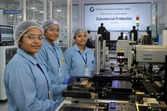
Prime Minister Narendra Modi inaugurated commercial production at CG Semi’s outsourced semiconductor assembly and test facility in Sanand, Gujarat, on July 4, 2026, marking the latest operational plant under the India Semiconductor Mission and adding another packaging-and-testing node to India’s emerging chip-manufacturing map. The event, reported by The News Mill and corroborated by Business Standard, Moneycontrol, the Press Information Bureau, and other Indian outlets, is being framed by New Delhi as proof that India’s semiconductor program has moved from memorandum to machinery. That framing is not wrong, but it is incomplete. Sanand is now important not because India has suddenly caught Taiwan, South Korea, or the United States, but because the country is finally building the industrial middle layer that makes modern electronics supply chains real.
The temptation around any semiconductor ribbon-cutting is to talk as if a nation has entered the chip big leagues the moment a cleanroom opens. That is especially true in India, where the political narrative around semiconductors has been inseparable from national capability, strategic autonomy, and the desire to move up from software and services into hard-tech manufacturing. The CG Semi inauguration feeds that story neatly: a large investment, a global joint venture, a named industrial cluster, and a Prime Ministerial visit.
But the more useful way to read Sanand is less cinematic and more industrial. CG Semi’s site is an OSAT facility, which means it handles outsourced semiconductor assembly and test. In plain terms, it takes fabricated silicon dies and turns them into usable components through packaging, inspection, testing, and qualification.
That distinction matters. India is not suddenly manufacturing the most advanced logic chips from raw wafers at scale in Gujarat. It is building capacity in the part of the value chain that makes chips usable in phones, cars, industrial equipment, telecom gear, power systems, and PCs. For WindowsForum readers, this is the layer that sits between chip design and the devices that eventually land on a desk, in a server rack, or inside an embedded controller running Windows IoT.
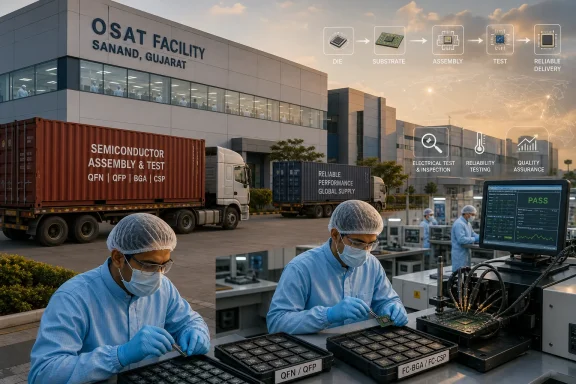
CG Semi says the facility will produce legacy packages such as QFN and QFP, as well as more advanced forms including FC-BGA and FC-CSP. Those acronyms are not marketing confetti. They describe packaging technologies used across everything from microcontrollers and power-management devices to higher-density chips where thermal behavior, electrical performance, and board space all matter.
That is why the plant is more consequential than a simple “India makes chips” headline suggests. The semiconductor world is no longer just about who etches the smallest transistor. Increasingly, packaging determines whether multiple dies can work together efficiently, whether a chip can dissipate heat, and whether a system can meet cost and reliability targets in the real world.
Commercial production in July 2026 means the project moved from approval to operations in a little under two and a half years. In semiconductor infrastructure, that is not trivial. Even packaging facilities require specialized equipment, process engineering, utilities, quality systems, supply contracts, trained workers, and customer qualification.
Business Standard reported that CG Semi’s G1 OSAT facility has begun commercial production, while Moneycontrol reported that the plant had already started exporting assembled chips to Malaysia ahead of the formal ceremony. If that reporting holds up at scale, it points to something more meaningful than a ceremonial start: the plant is not merely built; it is entering customer-facing production.
That is the metric that matters. Semiconductor announcements are easy. Semiconductor qualification is brutal. Customers do not buy patriotic capacity; they buy parts that pass reliability tests, arrive on time, meet automotive or industrial tolerances where required, and do not break their own supply-chain promises downstream.
The government’s message is that India can now execute. Prime Minister Modi used the event to argue that the country is building a complete electronics value chain rather than a single factory. Union Minister Ashwini Vaishnaw, according to the Press Information Bureau, described the inauguration as a milestone in India’s semiconductor journey. Those are political formulations, but they rest on a real industrial question: can India make semiconductor manufacturing boring enough to be trusted?
In this business, boring is victory. A plant that quietly ships tested parts for years will matter more than a hundred launch speeches.
The comparison to Taiwan’s Hsinchu or South Korea’s Gyeonggi province is ambitious, perhaps too ambitious for now, but not meaningless. Semiconductor ecosystems are geographic creatures. They need suppliers, logistics, engineering talent, tool maintenance, chemical handling, packaging know-how, testing labs, clean power, water systems, customs workflows, and executives who can get from one customer meeting to another without turning every operational issue into a national project.
Sanand already had an industrial base as an automobile hub. That matters because auto manufacturing leaves behind more than factories. It creates vendor networks, warehousing capacity, labor familiarity with quality systems, and government experience with land, permits, utilities, and logistics. Semiconductors are more exacting, but they do not grow from empty fields.
The clustering effect is now visible. Micron’s ATMP facility, Kaynes Semicon’s OSAT facility, and CG Semi’s plant give Sanand a concentration of chip packaging and testing activity that India did not previously have. The first phase of a semiconductor ecosystem often looks less like a gleaming fab and more like a series of pragmatic adjacency bets.
That may disappoint anyone looking for India’s immediate answer to TSMC. It should not. Assembly, test, and packaging are precisely where a country trying to enter the global semiconductor chain can build operational discipline, train workers, develop supplier relationships, and earn customer confidence before claiming a larger share of the stack.
OSAT facilities sit in that underappreciated middle. They receive wafers or dies, assemble them into packages, connect them to the outside world, test their electrical behavior, screen for failures, and prepare them for shipment. In many applications, especially automotive and industrial systems, packaging reliability can be as important as raw compute performance.
That is one reason India’s entry through OSAT and ATMP facilities is strategically coherent. The country already has electronics demand, design talent, and a policy desire to localize more of the production chain. Packaging gives India a way to connect those strengths to global supply chains without pretending that it can replicate decades of advanced-node process technology overnight.
There is also a deeper industry trend in India’s favor. Advanced packaging is becoming more valuable as chipmakers move beyond monolithic designs. Chiplets, heterogeneous integration, high-bandwidth memory stacks, and complex substrates make packaging a frontier technology rather than a back-office function. FC-BGA and FC-CSP capabilities are not enough by themselves to put India at the top of that frontier, but they put Indian facilities in the conversation.
For PC and server buyers, the connection is indirect but real. The reliability of the global electronics ecosystem depends on where components are assembled, tested, and qualified. A more distributed packaging base can reduce bottlenecks, diversify sourcing, and give OEMs more flexibility when shocks hit East Asian supply chains.
That does not mean the next Windows laptop will suddenly become “Indian-made” because CG Semi is online. It means the component chain feeding laptops, desktops, networking gear, industrial PCs, and edge devices could gradually become less geographically concentrated.
Malaysia is itself a major semiconductor packaging and testing hub, so shipping assembled chips there is not simply a matter of finding an easy overseas buyer. It suggests CG Semi is plugging into existing regional supply networks rather than operating as an isolated domestic showcase. That is what India needs if its semiconductor mission is to become durable.
The challenge is that semiconductor supply chains are conservative for good reasons. Customers qualify parts and suppliers slowly because failures can be expensive, dangerous, or reputation-destroying. Automotive chips, power devices, telecom components, and industrial electronics all carry reliability expectations that are harder to satisfy than consumer-gadget hype cycles imply.
If CG Semi can maintain yields, pass audits, and expand product coverage, the Sanand plant becomes a proof point for other investors. If production stumbles, the same facility will be used by skeptics as evidence that India’s semiconductor ambitions are still ahead of its manufacturing base. The stakes are asymmetric because early projects carry the burden of national expectation.
That is why the next two years matter more than the inauguration week. Hiring targets, export volumes, defect rates, customer wins, and the pace of the second CG Semi plant will tell us whether Sanand is becoming an ecosystem or merely a cluster of subsidized assets.
The company and state officials have discussed the combined capacity of two CG Semi facilities reaching 15 million chips per day. Capacity announcements, however, are not the same as utilized, revenue-generating output. The semiconductor industry is littered with nameplate numbers that looked impressive until demand, yield, or qualification reality intervened.
The CG Semi joint venture shows that clearly. Renesas brings semiconductor product and market experience. Stars Microelectronics brings OSAT know-how. CG Power brings domestic industrial grounding and local execution. This is not autarky; it is globalization with an Indian address.
That distinction is important because semiconductor independence is mostly a myth. Even the United States, Taiwan, South Korea, Japan, the Netherlands, and Germany depend on one another for equipment, materials, design software, wafers, gases, chemicals, substrates, and specialized talent. The goal is not to own everything. The goal is to own enough important nodes that a country cannot be ignored.
India’s advantage is demand. It has a large electronics market, a growing automotive sector, expanding telecom infrastructure, and a strategic desire to manufacture more of what it consumes. Its disadvantage is that semiconductor manufacturing ecosystems are unforgiving. They reward accumulated process knowledge, supplier density, and quality culture more than headline investment totals.
This is where the India Semiconductor Mission 2.0 language becomes relevant. The government has signaled that the next phase will focus more heavily on materials, components, equipment, and the surrounding industrial base. That is the correct direction. A packaging plant without substrates, gases, chemicals, precision tooling, maintenance capability, and skilled technicians nearby is still dependent on imported industrial oxygen.
The broader opportunity for Indian companies may not be only in chips themselves. It may be in the less glamorous businesses around them: specialty logistics, cleanroom services, testing equipment support, substrate supply, chemicals, automation, power systems, and workforce training. Those are not the sectors that win national slogans, but they are the sectors that make a semiconductor cluster stick.
But the Windows ecosystem is deeply exposed to semiconductor geography. PCs rely on processors, memory, storage controllers, display drivers, Wi-Fi modules, embedded controllers, sensors, power chips, and security components. Servers and workstations add even more dependency on networking silicon, power delivery, accelerators, and board-level reliability.
The pandemic-era shortages taught the industry that the problem is not always the glamorous processor. Sometimes the missing part is a low-cost microcontroller, a power regulator, or a packaging bottleneck that prevents an otherwise finished component from shipping. OSAT capacity is one of the pressure points that can determine whether hardware reaches OEMs on schedule.
For enterprise IT, that matters because hardware lead times translate into deployment delays, refresh-cycle uncertainty, and higher procurement costs. A more geographically diversified packaging base will not eliminate shortages, but it can reduce single-region risk. India’s emergence as a packaging and test location gives global OEMs another option in long-term supply-chain planning.
There is also a software angle. As India’s electronics-manufacturing base deepens, more industrial and embedded Windows deployments may be designed closer to domestic hardware supply. Factories, testing labs, automation systems, and logistics hubs all consume PCs, servers, ruggedized devices, and management software. Semiconductor manufacturing does not just produce chips; it consumes an enormous amount of IT infrastructure.
For Microsoft, Intel, AMD, Qualcomm, Dell, HP, Lenovo, and the broader Windows hardware world, India’s semiconductor buildout is less about immediate substitution and more about ecosystem gravity. The more electronics manufacturing clusters in India, the more local demand there will be for engineering workstations, endpoint management, device security, cloud integration, and industrial software.
There is also a risk in reducing every semiconductor investment to political theater. The CG Semi facility is not imaginary. It has named international partners, an approved investment structure, reported exports, an operational production launch, and a place in a growing local cluster. Those are tangible facts.
The better critique is not that the project is meaningless, but that its success should be measured by industrial outcomes rather than ceremonial optics. How many customers qualify the plant? How much output is exported? How quickly does the second plant come online? How much of the input supply chain localizes? How many technicians and process engineers stay in the sector after the first wave of hiring?
Those questions are less emotionally satisfying than slogans about silicon sovereignty, but they are the ones that will determine whether Sanand becomes a durable node in the global electronics map. Semiconductor ecosystems are built through compounding reliability. Each successful shipment makes the next customer easier to win.
The comparison to Hsinchu and Gyeonggi should therefore be treated as aspiration, not conclusion. Those regions became powerful because universities, suppliers, state policy, global customers, and private companies reinforced one another over decades. Gujarat has made an impressive start, but semiconductor history is written in production runs, not press conferences.
The second lesson is that partnerships matter. India’s semiconductor ambitions are strongest where domestic industrial groups work with experienced international firms rather than trying to invent every capability from scratch. The CG Semi-Renesas-Stars structure reflects that reality.
The third lesson is that clusters beat isolated plants. Sanand’s advantage is not one facility but the accumulation of Micron, Kaynes, CG Semi, and other approved projects around a state government that has made semiconductors a policy priority. If suppliers and talent follow, the cluster becomes more valuable than the sum of its announcements.
The fourth lesson is that the next bottleneck will be inputs. Materials, substrates, specialty chemicals, gases, tools, maintenance services, and trained people will decide whether India can move from assembly capacity to ecosystem resilience. India Semiconductor Mission 2.0 appears designed to address that gap, but execution will be harder than allocation.
 Sanand Is Becoming India’s Packaging Bet, Not Its Silicon Valley Overnight
The temptation around any semiconductor ribbon-cutting is to talk as if a nation has entered the chip big leagues the moment a cleanroom opens. That is especially true in India, where the political narrative around semiconductors has been inseparable from national capability, strategic autonomy, and the desire to move up from software and services into hard-tech manufacturing. The CG Semi inauguration feeds that story neatly: a large investment, a global joint venture, a named industrial cluster, and a Prime Ministerial visit.But the more useful way to read Sanand is less cinematic and more industrial. CG Semi’s site is an OSAT facility, which means it handles outsourced semiconductor assembly and test. In plain terms, it takes fabricated silicon dies and turns them into usable components through packaging, inspection, testing, and qualification.
That distinction matters. India is not suddenly manufacturing the most advanced logic chips from raw wafers at scale in Gujarat. It is building capacity in the part of the value chain that makes chips usable in phones, cars, industrial equipment, telecom gear, power systems, and PCs. For WindowsForum readers, this is the layer that sits between chip design and the devices that eventually land on a desk, in a server rack, or inside an embedded controller running Windows IoT.
CG Semi says the facility will produce legacy packages such as QFN and QFP, as well as more advanced forms including FC-BGA and FC-CSP. Those acronyms are not marketing confetti. They describe packaging technologies used across everything from microcontrollers and power-management devices to higher-density chips where thermal behavior, electrical performance, and board space all matter.
That is why the plant is more consequential than a simple “India makes chips” headline suggests. The semiconductor world is no longer just about who etches the smallest transistor. Increasingly, packaging determines whether multiple dies can work together efficiently, whether a chip can dissipate heat, and whether a system can meet cost and reliability targets in the real world.
The Real Story Is the Speed From Approval to Production
According to CG Power disclosures and government material, the Sanand OSAT project was approved by India’s Union Cabinet in February 2024 under the India Semiconductor Mission. CG Semi, a subsidiary of CG Power and Industrial Solutions, is backed by a joint venture involving Japan’s Renesas Electronics and Thailand’s Stars Microelectronics. The investment has been described at roughly ₹7,600 crore, spread over several years.Commercial production in July 2026 means the project moved from approval to operations in a little under two and a half years. In semiconductor infrastructure, that is not trivial. Even packaging facilities require specialized equipment, process engineering, utilities, quality systems, supply contracts, trained workers, and customer qualification.
Business Standard reported that CG Semi’s G1 OSAT facility has begun commercial production, while Moneycontrol reported that the plant had already started exporting assembled chips to Malaysia ahead of the formal ceremony. If that reporting holds up at scale, it points to something more meaningful than a ceremonial start: the plant is not merely built; it is entering customer-facing production.
That is the metric that matters. Semiconductor announcements are easy. Semiconductor qualification is brutal. Customers do not buy patriotic capacity; they buy parts that pass reliability tests, arrive on time, meet automotive or industrial tolerances where required, and do not break their own supply-chain promises downstream.
The government’s message is that India can now execute. Prime Minister Modi used the event to argue that the country is building a complete electronics value chain rather than a single factory. Union Minister Ashwini Vaishnaw, according to the Press Information Bureau, described the inauguration as a milestone in India’s semiconductor journey. Those are political formulations, but they rest on a real industrial question: can India make semiconductor manufacturing boring enough to be trusted?
In this business, boring is victory. A plant that quietly ships tested parts for years will matter more than a hundred launch speeches.
Gujarat Has Turned Industrial Policy Into Geographic Momentum
Sanand’s rise is not accidental. Gujarat was among the first Indian states to create a dedicated semiconductor policy, and the state has aggressively positioned itself as the natural home for chip-related projects. The News Mill notes that Gujarat now hosts multiple approved semiconductor projects, including Tata Electronics, Micron Technology, CG Semi, Kaynes Semicon, Suchi Semicon, and Crystal Matrix.The comparison to Taiwan’s Hsinchu or South Korea’s Gyeonggi province is ambitious, perhaps too ambitious for now, but not meaningless. Semiconductor ecosystems are geographic creatures. They need suppliers, logistics, engineering talent, tool maintenance, chemical handling, packaging know-how, testing labs, clean power, water systems, customs workflows, and executives who can get from one customer meeting to another without turning every operational issue into a national project.
Sanand already had an industrial base as an automobile hub. That matters because auto manufacturing leaves behind more than factories. It creates vendor networks, warehousing capacity, labor familiarity with quality systems, and government experience with land, permits, utilities, and logistics. Semiconductors are more exacting, but they do not grow from empty fields.
The clustering effect is now visible. Micron’s ATMP facility, Kaynes Semicon’s OSAT facility, and CG Semi’s plant give Sanand a concentration of chip packaging and testing activity that India did not previously have. The first phase of a semiconductor ecosystem often looks less like a gleaming fab and more like a series of pragmatic adjacency bets.
That may disappoint anyone looking for India’s immediate answer to TSMC. It should not. Assembly, test, and packaging are precisely where a country trying to enter the global semiconductor chain can build operational discipline, train workers, develop supplier relationships, and earn customer confidence before claiming a larger share of the stack.
Packaging Is Where the Chip War Gets Less Glamorous and More Important
For years, the public conversation about semiconductors has been dominated by leading-edge fabrication: 3-nanometer, 2-nanometer, EUV lithography, AI accelerators, and the geopolitical importance of Taiwan. That focus is understandable, but it hides the rest of the machine. A chip that has been fabricated but not packaged and tested is not a product.OSAT facilities sit in that underappreciated middle. They receive wafers or dies, assemble them into packages, connect them to the outside world, test their electrical behavior, screen for failures, and prepare them for shipment. In many applications, especially automotive and industrial systems, packaging reliability can be as important as raw compute performance.
That is one reason India’s entry through OSAT and ATMP facilities is strategically coherent. The country already has electronics demand, design talent, and a policy desire to localize more of the production chain. Packaging gives India a way to connect those strengths to global supply chains without pretending that it can replicate decades of advanced-node process technology overnight.
There is also a deeper industry trend in India’s favor. Advanced packaging is becoming more valuable as chipmakers move beyond monolithic designs. Chiplets, heterogeneous integration, high-bandwidth memory stacks, and complex substrates make packaging a frontier technology rather than a back-office function. FC-BGA and FC-CSP capabilities are not enough by themselves to put India at the top of that frontier, but they put Indian facilities in the conversation.
For PC and server buyers, the connection is indirect but real. The reliability of the global electronics ecosystem depends on where components are assembled, tested, and qualified. A more distributed packaging base can reduce bottlenecks, diversify sourcing, and give OEMs more flexibility when shocks hit East Asian supply chains.
That does not mean the next Windows laptop will suddenly become “Indian-made” because CG Semi is online. It means the component chain feeding laptops, desktops, networking gear, industrial PCs, and edge devices could gradually become less geographically concentrated.
The Export Claim Is the Quiet Signal Investors Should Watch
Moneycontrol’s report that CG Semi had already begun exporting assembled chips to Malaysia before the formal launch may be the most important detail in the entire story. Domestic political ceremonies prove government support. Exports prove customer acceptance.Malaysia is itself a major semiconductor packaging and testing hub, so shipping assembled chips there is not simply a matter of finding an easy overseas buyer. It suggests CG Semi is plugging into existing regional supply networks rather than operating as an isolated domestic showcase. That is what India needs if its semiconductor mission is to become durable.
The challenge is that semiconductor supply chains are conservative for good reasons. Customers qualify parts and suppliers slowly because failures can be expensive, dangerous, or reputation-destroying. Automotive chips, power devices, telecom components, and industrial electronics all carry reliability expectations that are harder to satisfy than consumer-gadget hype cycles imply.
If CG Semi can maintain yields, pass audits, and expand product coverage, the Sanand plant becomes a proof point for other investors. If production stumbles, the same facility will be used by skeptics as evidence that India’s semiconductor ambitions are still ahead of its manufacturing base. The stakes are asymmetric because early projects carry the burden of national expectation.
That is why the next two years matter more than the inauguration week. Hiring targets, export volumes, defect rates, customer wins, and the pace of the second CG Semi plant will tell us whether Sanand is becoming an ecosystem or merely a cluster of subsidized assets.
The company and state officials have discussed the combined capacity of two CG Semi facilities reaching 15 million chips per day. Capacity announcements, however, are not the same as utilized, revenue-generating output. The semiconductor industry is littered with nameplate numbers that looked impressive until demand, yield, or qualification reality intervened.
India’s Chip Strategy Is a Supply-Chain Strategy Wearing a Sovereignty Suit
New Delhi’s language around semiconductors often invokes sovereignty, self-reliance, and national technological destiny. That is politically potent, but the practical strategy is more supply-chain oriented. India wants to become useful to the world’s electronics industry, not merely independent from it.The CG Semi joint venture shows that clearly. Renesas brings semiconductor product and market experience. Stars Microelectronics brings OSAT know-how. CG Power brings domestic industrial grounding and local execution. This is not autarky; it is globalization with an Indian address.
That distinction is important because semiconductor independence is mostly a myth. Even the United States, Taiwan, South Korea, Japan, the Netherlands, and Germany depend on one another for equipment, materials, design software, wafers, gases, chemicals, substrates, and specialized talent. The goal is not to own everything. The goal is to own enough important nodes that a country cannot be ignored.
India’s advantage is demand. It has a large electronics market, a growing automotive sector, expanding telecom infrastructure, and a strategic desire to manufacture more of what it consumes. Its disadvantage is that semiconductor manufacturing ecosystems are unforgiving. They reward accumulated process knowledge, supplier density, and quality culture more than headline investment totals.
This is where the India Semiconductor Mission 2.0 language becomes relevant. The government has signaled that the next phase will focus more heavily on materials, components, equipment, and the surrounding industrial base. That is the correct direction. A packaging plant without substrates, gases, chemicals, precision tooling, maintenance capability, and skilled technicians nearby is still dependent on imported industrial oxygen.
The broader opportunity for Indian companies may not be only in chips themselves. It may be in the less glamorous businesses around them: specialty logistics, cleanroom services, testing equipment support, substrate supply, chemicals, automation, power systems, and workforce training. Those are not the sectors that win national slogans, but they are the sectors that make a semiconductor cluster stick.
Windows Hardware Will Feel This Slowly, Then All at Once
Windows users are unlikely to see an immediate product label that says a CG Semi package sits inside their next desktop motherboard. Semiconductor supply chains are too layered for that. A power-management chip, microcontroller, RF component, or industrial controller may pass through multiple hands before it becomes part of a branded device.But the Windows ecosystem is deeply exposed to semiconductor geography. PCs rely on processors, memory, storage controllers, display drivers, Wi-Fi modules, embedded controllers, sensors, power chips, and security components. Servers and workstations add even more dependency on networking silicon, power delivery, accelerators, and board-level reliability.
The pandemic-era shortages taught the industry that the problem is not always the glamorous processor. Sometimes the missing part is a low-cost microcontroller, a power regulator, or a packaging bottleneck that prevents an otherwise finished component from shipping. OSAT capacity is one of the pressure points that can determine whether hardware reaches OEMs on schedule.
For enterprise IT, that matters because hardware lead times translate into deployment delays, refresh-cycle uncertainty, and higher procurement costs. A more geographically diversified packaging base will not eliminate shortages, but it can reduce single-region risk. India’s emergence as a packaging and test location gives global OEMs another option in long-term supply-chain planning.
There is also a software angle. As India’s electronics-manufacturing base deepens, more industrial and embedded Windows deployments may be designed closer to domestic hardware supply. Factories, testing labs, automation systems, and logistics hubs all consume PCs, servers, ruggedized devices, and management software. Semiconductor manufacturing does not just produce chips; it consumes an enormous amount of IT infrastructure.
For Microsoft, Intel, AMD, Qualcomm, Dell, HP, Lenovo, and the broader Windows hardware world, India’s semiconductor buildout is less about immediate substitution and more about ecosystem gravity. The more electronics manufacturing clusters in India, the more local demand there will be for engineering workstations, endpoint management, device security, cloud integration, and industrial software.
The Hype Should Be Resisted Because the Milestone Is Real Enough
There is a danger in overclaiming Sanand. India still does not have the depth of fabrication capacity, equipment supply, advanced materials, and decades of process learning that define the world’s dominant semiconductor regions. Packaging plants are critical, but they are not the same as leading-edge fabs. Commercial production is a start, not a coronation.There is also a risk in reducing every semiconductor investment to political theater. The CG Semi facility is not imaginary. It has named international partners, an approved investment structure, reported exports, an operational production launch, and a place in a growing local cluster. Those are tangible facts.
The better critique is not that the project is meaningless, but that its success should be measured by industrial outcomes rather than ceremonial optics. How many customers qualify the plant? How much output is exported? How quickly does the second plant come online? How much of the input supply chain localizes? How many technicians and process engineers stay in the sector after the first wave of hiring?
Those questions are less emotionally satisfying than slogans about silicon sovereignty, but they are the ones that will determine whether Sanand becomes a durable node in the global electronics map. Semiconductor ecosystems are built through compounding reliability. Each successful shipment makes the next customer easier to win.
The comparison to Hsinchu and Gyeonggi should therefore be treated as aspiration, not conclusion. Those regions became powerful because universities, suppliers, state policy, global customers, and private companies reinforced one another over decades. Gujarat has made an impressive start, but semiconductor history is written in production runs, not press conferences.
The Sanand Lesson Is That India Is Learning Where to Enter the Stack
The most concrete lesson from CG Semi’s launch is that India has chosen a plausible entry point. OSAT and ATMP facilities are not consolation prizes. They are essential parts of the semiconductor economy and increasingly strategic as packaging grows more complex.The second lesson is that partnerships matter. India’s semiconductor ambitions are strongest where domestic industrial groups work with experienced international firms rather than trying to invent every capability from scratch. The CG Semi-Renesas-Stars structure reflects that reality.
The third lesson is that clusters beat isolated plants. Sanand’s advantage is not one facility but the accumulation of Micron, Kaynes, CG Semi, and other approved projects around a state government that has made semiconductors a policy priority. If suppliers and talent follow, the cluster becomes more valuable than the sum of its announcements.
The fourth lesson is that the next bottleneck will be inputs. Materials, substrates, specialty chemicals, gases, tools, maintenance services, and trained people will decide whether India can move from assembly capacity to ecosystem resilience. India Semiconductor Mission 2.0 appears designed to address that gap, but execution will be harder than allocation.
The Chip Cluster’s Real Scorecard Starts After the Cameras Leave
The next phase of this story will be measured less by political ceremony and more by industrial repetition. These are the markers that will show whether CG Semi’s Sanand plant is becoming a durable semiconductor asset rather than a one-week headline.- CG Semi must demonstrate sustained commercial output, not just nameplate capacity or ceremonial production.
- Customer qualification and export growth will matter more than domestic announcements.
- The second CG Semi plant will test whether the company can scale beyond a successful first phase.
- Gujarat’s semiconductor cluster will need local suppliers, trained technicians, and reliable utilities to become more than a group of subsidized factories.
- India’s broader chip strategy will depend on whether OSAT momentum can pull in materials, components, equipment support, and eventually deeper manufacturing capability.
- Windows hardware buyers will feel the impact indirectly through supply-chain diversification, procurement resilience, and the long-term geography of electronics manufacturing.
References
- Primary source: The News Mill
Published: Sun, 05 Jul 2026 07:17:49 GMT
PM Modi inaugurates semiconductor production in Sanand, Gujarat
On July 4, PM Modi will launch CG Semi's OSAT facility in Sanand, Gujarat, boosting semiconductor production capacity to 15 million chips daily.thenewsmill.com - Related coverage: business-standard.com
- Related coverage: moneycontrol.com
PM Modi inaugurates commercial production at CG Semi's Sanand semiconductor facility
"The Semicon India programme is gathering rapid momentum... Step by step. Brick by brick. Chip by chip," PM Modi said.www.moneycontrol.com - Related coverage: deshgujarat.com
PM Modi in Gujarat, inaugurates CG Semi OSAT facility in Sanand | DeshGujarat
Sanand: Prime Minister Narendra Modi today inaugurated the CG Semi Outsourced Semiconductor Assembly and Test (OSAT) facility in Sanand, Gujarat. Highlighting the significance of the deshgujarat.com
- Related coverage: opindia.com
PM Modi inaugurates CG Semi Outsourced Semiconductor Assembly and Test facility in Sanand
Prime Minister Narendra Modi today inaugurated the CG Semi Outsourced Semiconductor Assembly and Test (OSAT) facility in Sanand, Gujarat, formally www.opindia.com
- Related coverage: nationpress.com
PM Modi Inaugurates CG Semi OSAT Facility in Sanand | Nation Press
Prime Minister Narendra Modi inaugurated the CG Semi OSAT facility in Sanand, Gujarat on 4 July 2026, advancing India's domestic semiconductor assembly and testing capacity under the India Semiconductor Mission launched in 2021.www.nationpress.com
- Related coverage: newsinc24.com
Gujarat:PM Modi inaugurates the CG Semi OSAT facility in Sanand
The launch marks the transition of the Sanand plant from the commissioning stage to full commercial operations.www.newsinc24.com - Related coverage: economictimes.indiatimes.com
PM Modi inaugurates CG Semi chip plant in Sanand, Gujarat - The Economic Times
Prime Minister Narendra Modi inaugurated India's third semiconductor manufacturing plant in Sanand, Gujarat, a significant stride in building a domestic chip ecosystem. This facility aims to bolster manufacturing, strengthen electronics supply chains, and reduce import reliance. Union Minister...economictimes.indiatimes.com
- Related coverage: timesofindia.indiatimes.com
PM to inaugurate CG Semi’s Rs 7,500 cr facility in Sanand today | Ahmedabad News - The Times of India
PM Narendra Modi inaugurates CG Semi’s ₹7,500-crore OSAT chip assembly and test plant in Sanand, launching commercial production under India Semiconductor Mission.timesofindia.indiatimes.com - Related coverage: niti.gov.in