

Researchers at POSTECH and KITECH have demonstrated a packaging process that stably stacks more than 10 silicon chips, each approximately 14 micrometers thick, under temperatures below 180°C and pressures below 20 kPa. The reported integration density is approximately four times that of the conventional 12-layer high-bandwidth-memory structure used as the benchmark.
That does not mean AI systems are about to receive four times the memory bandwidth, four times the capacity, or four times the performance. Nor is the research a production-ready replacement for commercial HBM. Its significance is at the packaging level: it demonstrates a combined transfer-printing and in-situ-bonding process for repeatedly assembling ultrathin silicon under relatively mild conditions.
This article is based on Tech Xplore’s July 8, 2026 report, “AI memory bottleneck may ease as ultrathin chip stacks quadruple high-bandwidth memory density,” and the underlying paper by Uhyeon Kim and colleagues, “Transfer Printing and In-Situ Bonding for Ultra-High-Density Integration,” published in Results in Engineering under DOI 10.1016/j.rineng.2026.111194.
The popular explanation for AI performance is usually computational: larger models need more accelerators, faster arithmetic, and more electrical power. But accelerators remain dependent on memory systems that can store and deliver data at sufficient speed. That is why high-bandwidth memory has become a defining component of modern AI infrastructure.
HBM addresses the data-delivery problem by stacking memory dies vertically and placing them close to the processor. Instead of expanding only across a circuit board, manufacturers use the third dimension to fit multiple memory layers into a compact package.
That architectural decision does not eliminate engineering constraints. It shifts more of the challenge into semiconductor packaging. As stacks become more ambitious, manufacturers must control die handling, placement, bonding, package height, thermal behavior, and the cumulative effect of repeating assembly operations across many layers.
The research reported by Tech Xplore addresses this physical side of semiconductor scaling. The work was conducted by a team led by Prof. Seok Kim and integrated Ph.D. student Uhyeon Kim of POSTECH’s Department of Mechanical Engineering, together with Dr. Hohyun Keum of the Korea Institute of Industrial Technology.
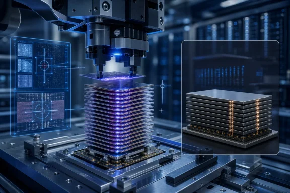
The researchers combined transfer printing with in-situ bonding in one platform. The process transfers an ultrathin chip to its intended position while also forming the connection needed to add it to the stack. Using this approach, the team assembled more than 10 chips at temperatures below 180°C and pressures below 20 kPa.
The central result is therefore not the invention of vertical stacking. Semiconductor manufacturers already use vertical integration in commercial memory and other advanced packages. The contribution is a process for transferring and bonding unusually thin silicon repeatedly, allowing more layers to fit within a constrained vertical space.
At approximately 14 μm, a chip is only about one-fifth the thickness of a human hair. At that scale, the material cannot be treated exactly like a conventional, thicker die during assembly. The manufacturing process must maintain control while moving, positioning, and bonding each layer.
Thickness is therefore not a free scaling lever. It is not enough to make dies thinner and assume that an existing production flow can stack proportionally more of them. The assembly method must be capable of handling the resulting structures consistently, particularly when the operation is repeated across a multilayer package.
This is what makes the reported demonstration relevant. The team did not stop after fabricating one thin chip or completing a single transfer. It used the integrated process to build a stack containing more than 10 approximately 14 μm chips.
The research establishes that such repeated stacking can be performed under the reported laboratory conditions. It does not establish that the same process already meets the speed, yield, cost, and long-term reliability requirements of a commercial memory production line.
The practical point is process integration. Chip transfer, positioning, and bonding are performed as parts of a combined workflow instead of being presented as wholly separate stages.
That approach is well matched to the objective of repeated ultrathin-chip assembly. The process must not only move each layer into place but also add it to an increasingly tall structure. The team demonstrated that this sequence could be repeated more than 10 times while using the stated low-temperature and low-pressure conditions.
The study is about a research-scale integration platform rather than a finished HBM device. The fabricated structures serve as a way to test whether the transfer-and-bond concept can support dense multilayer integration. They should not be interpreted as commercially qualified memory dies or as a complete replacement for the electrical architecture of HBM.
The comparison shows why the density result needs careful interpretation. The researchers did not demonstrate four times as many layers as a 12-layer HBM stack. Rather, the use of much thinner chips allowed the experimental structure to achieve a substantially higher reported level of vertical integration.
The result does not by itself establish:
The distinction does not make the research unimportant. Vertical space is a real packaging constraint, and a method that fits more silicon into a given package height could create new options for memory and heterogeneous integration. It could eventually contribute to packages with more capacity or a different combination of functional layers.
Density is nevertheless an enabling metric, not a complete product specification. Commercial HBM is valuable because it delivers defined capacity and bandwidth while meeting electrical, thermal, mechanical, manufacturing, and reliability requirements. A laboratory platform can improve one packaging metric without yet matching the full capabilities of a shipping memory subsystem.
Prof. Seok Kim described the technology as a potential enabling technology for future high-performance AI semiconductors and next-generation memory. “Enabling” is the appropriate term. The work presents a possible route toward denser integration; it does not establish that the AI memory bottleneck has been solved.
The significance should be stated narrowly. The researchers showed that stable stacking of more than 10 ultrathin chips could be achieved without requiring higher temperatures or pressures than the reported limits. That supports the case for a comparatively gentle assembly method.
It does not, on its own, prove compatibility with every semiconductor material, foundry process, memory design, or commercial packaging line. Manufacturers would have to test the process with the specific devices, metals, substrates, interfaces, and production equipment intended for a product.
A packaging technique must also remain effective outside a controlled demonstration. Commercialization would require evidence that process conditions can be maintained across many packages, manufacturing lots, tools, and facilities.
The research supplies a credible starting point for that work. It shows that chip transfer, placement, bonding, and repeated stacking can be integrated under the reported conditions. The next stage would be proving that the process window is wide and repeatable enough for industrial use.
Chiplets allow designers to combine separately manufactured dies within a larger package. In principle, that provides flexibility to mix compute, memory, communications, analog, or specialized accelerator functions without manufacturing every element on one monolithic die.
Assembly remains one of the key challenges. Components must be positioned and connected within the electrical, physical, and thermal limits of the package. A process designed to transfer and bond ultrathin silicon could eventually give packaging engineers another integration option.
That is a plausible direction rather than a product forecast. Adoption would depend on whether transfer printing offers a measurable advantage over established and emerging packaging techniques for a particular chiplet design.
The necessary evidence would include placement throughput, connection density, electrical performance, process repeatability, supported die sizes, equipment cost, and compatibility with the rest of the assembly flow.
Dr. Hohyun Keum said the micrometer-scale alignment and bonding technologies could be applied broadly to next-generation semiconductor and display manufacturing. That statement identifies a field of potential application. It should not be read as confirmation that a display or chiplet manufacturer has selected the process for production.
A research platform can demonstrate that an operation is physically possible. A semiconductor factory must determine whether it can be repeated rapidly, consistently, and economically.
Production equipment would need to transfer and bond chips at a throughput appropriate for the target market. The process would need to remain stable across extended operation and ordinary variation in incoming materials. Manufacturers would also need process controls capable of identifying a problem before additional value is added to a defective package.
Yield deserves particular attention. A multilayer package contains repeated process steps, and each step creates another opportunity for the final assembly to fall outside specifications. The commercial calculation depends on the percentage of completed stacks that pass all required tests, not merely on whether an individual chip can be transferred successfully.
The paper’s stacking result does not provide enough public evidence to calculate a production yield or cost per completed package. It also does not establish how quickly a production machine could perform the sequence. Any claim that the process will make memory cheaper, increase factory output, or improve commercial yield would therefore be premature.
The same caution applies to inspection. Manufacturers would need suitable methods for checking completed and partially completed structures, but the preferred inspection workflow would depend on the final package and production implementation. It is too early to prescribe a specific inspection system from this demonstration alone.
Long-term reliability testing would need to be matched to the intended product and operating environment. A data-center accelerator, automotive component, consumer device, and industrial controller do not necessarily face identical qualification requirements.
Manufacturers and customers would want to know whether a finished package continues to meet its specifications after sustained use and the environmental tests required for its market. Public product-level qualification data would be necessary before the process could be evaluated alongside mature commercial memory packaging.
Thermal behavior is another unresolved system question. Thinner chips reduce the height occupied by each layer, but the heat generated by a future product would depend on the circuits placed in the stack and how they operate.
It is reasonable to ask whether fitting more active layers into a similar volume would make cooling more demanding. The current density result, however, does not provide a complete thermal specification for a commercial memory product. Any conclusion about operating temperatures, cooling requirements, or power efficiency must wait for an actual device implementation.
The most accurate interpretation is that the researchers have advanced one part of the integration problem. They demonstrated a process for repeatedly transferring and bonding ultrathin chips. Product developers would still have to engineer and validate the complete electrical, thermal, mechanical, and manufacturing system around it.
HBM is primarily used with high-performance accelerators and specialized computing hardware. Mainstream PCs use different memory arrangements selected for their own balance of cost, capacity, performance, power, and serviceability.
The relevance to Windows users is upstream. Windows applications increasingly use AI services running locally, in data centers, or through a combination of both. The capabilities and economics of those services are affected by the memory available to their accelerators.
If ultrathin stacking eventually enables commercial memory with more usable capacity or a more efficient package design, future AI systems could benefit. The scale and nature of that benefit would depend on the specifications of the resulting products—not the packaging-density figure in isolation.
For IT departments, the broader lesson is that accelerator planning should not be reduced to processor counts or headline arithmetic performance. Memory capacity, bandwidth, power, cooling, software support, and deployment economics all influence the useful output of an AI system.
This research may eventually change some of those constraints. It does not yet provide procurement data, platform compatibility, availability dates, prices, or guaranteed application-performance gains.
Before treating this technique—or a related commercial implementation—as a product-level advance, track the following:
Advanced semiconductor packaging increasingly determines what can be built from separately fabricated components. A successful package must place and connect its elements while staying within strict physical, electrical, thermal, and manufacturing constraints.
The POSTECH-KITECH team demonstrated that an ultrathin chip can be transferred, positioned, and bonded as part of a repeatable stacking sequence. More than 10 chips were assembled under the reported low-temperature and low-pressure conditions, resulting in a much denser experimental structure than the commercial HBM benchmark used in the comparison.
That is a meaningful packaging achievement. It is also only one stage on the path from research to production.
Continue evaluating current systems according to measured workload performance, usable memory capacity, bandwidth, power, cooling, software compatibility, support, availability, and total cost of ownership.
At the same time, monitor whether semiconductor manufacturers announce commercial adoption of ultrathin transfer-and-bond packaging. Treat the technology as product-level progress only when vendors publish credible qualification and reliability results, bandwidth and capacity specifications, thermal data, manufacturing yield, and cost.
The fourfold figure is a packaging-density result—not fourfold bandwidth, capacity, AI speed, or a commercial HBM replacement. Its importance is forward-looking: it shows that combining transfer printing with in-situ bonding may give semiconductor engineers another way to build denser vertical structures.
Packaging is no longer merely the protective shell around the “real” chip. It increasingly determines how much silicon can be integrated, how closely components can be placed, and which system architectures are practical. The POSTECH-KITECH research belongs to that broader transition, where progress in AI hardware depends not only on better transistors but also on better ways to assemble them.
That does not mean AI systems are about to receive four times the memory bandwidth, four times the capacity, or four times the performance. Nor is the research a production-ready replacement for commercial HBM. Its significance is at the packaging level: it demonstrates a combined transfer-printing and in-situ-bonding process for repeatedly assembling ultrathin silicon under relatively mild conditions.
This article is based on Tech Xplore’s July 8, 2026 report, “AI memory bottleneck may ease as ultrathin chip stacks quadruple high-bandwidth memory density,” and the underlying paper by Uhyeon Kim and colleagues, “Transfer Printing and In-Situ Bonding for Ultra-High-Density Integration,” published in Results in Engineering under DOI 10.1016/j.rineng.2026.111194.
What changed—and what readers should do
Researchers demonstrated stable stacking of more than 10 approximately 14 μm silicon chips through a process that combines chip transfer, placement, and bonding. The result is a promising packaging advance, not a new HBM product. Readers and IT buyers should watch for commercial adoption, qualification data, memory specifications, thermals, manufacturing yield, and cost—not interpret the fourfold density figure as a fourfold system-performance claim.
 AI’s Memory Problem Is Becoming a Packaging Problem
The popular explanation for AI performance is usually computational: larger models need more accelerators, faster arithmetic, and more electrical power. But accelerators remain dependent on memory systems that can store and deliver data at sufficient speed. That is why high-bandwidth memory has become a defining component of modern AI infrastructure.HBM addresses the data-delivery problem by stacking memory dies vertically and placing them close to the processor. Instead of expanding only across a circuit board, manufacturers use the third dimension to fit multiple memory layers into a compact package.
That architectural decision does not eliminate engineering constraints. It shifts more of the challenge into semiconductor packaging. As stacks become more ambitious, manufacturers must control die handling, placement, bonding, package height, thermal behavior, and the cumulative effect of repeating assembly operations across many layers.
The research reported by Tech Xplore addresses this physical side of semiconductor scaling. The work was conducted by a team led by Prof. Seok Kim and integrated Ph.D. student Uhyeon Kim of POSTECH’s Department of Mechanical Engineering, together with Dr. Hohyun Keum of the Korea Institute of Industrial Technology.
The researchers combined transfer printing with in-situ bonding in one platform. The process transfers an ultrathin chip to its intended position while also forming the connection needed to add it to the stack. Using this approach, the team assembled more than 10 chips at temperatures below 180°C and pressures below 20 kPa.
The central result is therefore not the invention of vertical stacking. Semiconductor manufacturers already use vertical integration in commercial memory and other advanced packages. The contribution is a process for transferring and bonding unusually thin silicon repeatedly, allowing more layers to fit within a constrained vertical space.
At 14 Micrometers, Handling Becomes a Central Challenge
Semiconductor diagrams often depict chips as perfectly rigid slabs that can be lowered into position like tiles. That model becomes less useful as silicon is made extremely thin.At approximately 14 μm, a chip is only about one-fifth the thickness of a human hair. At that scale, the material cannot be treated exactly like a conventional, thicker die during assembly. The manufacturing process must maintain control while moving, positioning, and bonding each layer.
Thickness is therefore not a free scaling lever. It is not enough to make dies thinner and assume that an existing production flow can stack proportionally more of them. The assembly method must be capable of handling the resulting structures consistently, particularly when the operation is repeated across a multilayer package.
This is what makes the reported demonstration relevant. The team did not stop after fabricating one thin chip or completing a single transfer. It used the integrated process to build a stack containing more than 10 approximately 14 μm chips.
The research establishes that such repeated stacking can be performed under the reported laboratory conditions. It does not establish that the same process already meets the speed, yield, cost, and long-term reliability requirements of a commercial memory production line.
Transfer Printing Combines Placement With Bonding
Transfer printing uses a controlled transfer medium to pick up a small or thin component, move it, and release it at a target location. In the POSTECH-KITECH platform, that placement operation is paired with in-situ bonding.The practical point is process integration. Chip transfer, positioning, and bonding are performed as parts of a combined workflow instead of being presented as wholly separate stages.
That approach is well matched to the objective of repeated ultrathin-chip assembly. The process must not only move each layer into place but also add it to an increasingly tall structure. The team demonstrated that this sequence could be repeated more than 10 times while using the stated low-temperature and low-pressure conditions.
The study is about a research-scale integration platform rather than a finished HBM device. The fabricated structures serve as a way to test whether the transfer-and-bond concept can support dense multilayer integration. They should not be interpreted as commercially qualified memory dies or as a complete replacement for the electrical architecture of HBM.
| Packaging attribute | Conventional HBM benchmark | Research demonstration |
|---|---|---|
| Basic objective | Stack memory dies within a compact package | Explore denser multilayer integration using ultrathin silicon |
| Benchmark structure | Conventional 12-layer HBM structure | More than 10 chips stably stacked |
| Chip thickness | Established commercial packaging design | Approximately 14 μm |
| Assembly concept | Existing commercial fabrication and packaging flows | Transfer printing combined with in-situ bonding |
| Reported process conditions | Vary by manufacturer and product | Below 180°C and below 20 kPa |
| Reported density result | Baseline used by the researchers | Approximately four times higher integration density |
| Commercial status | Shipping memory technology | Laboratory research, not an announced HBM product |
The Fourfold Claim Is About Density, Not Instant Performance
“Four times higher than HBM” is a phrase that can quickly lose its engineering qualifiers. In this case, the reported advantage concerns integration density.The result does not by itself establish:
- Four times the memory bandwidth
- Four times the usable memory capacity
- Four times the AI training or inference speed
- One-quarter of the energy consumption
- Four times the number of commercially usable memory layers
- Compatibility with existing GPUs or HBM controllers
- A manufacturing cost comparable to current HBM
- A product ready for procurement or deployment
The distinction does not make the research unimportant. Vertical space is a real packaging constraint, and a method that fits more silicon into a given package height could create new options for memory and heterogeneous integration. It could eventually contribute to packages with more capacity or a different combination of functional layers.
Density is nevertheless an enabling metric, not a complete product specification. Commercial HBM is valuable because it delivers defined capacity and bandwidth while meeting electrical, thermal, mechanical, manufacturing, and reliability requirements. A laboratory platform can improve one packaging metric without yet matching the full capabilities of a shipping memory subsystem.
Prof. Seok Kim described the technology as a potential enabling technology for future high-performance AI semiconductors and next-generation memory. “Enabling” is the appropriate term. The work presents a possible route toward denser integration; it does not establish that the AI memory bottleneck has been solved.
Low Heat and Pressure Strengthen the Packaging Case
The team performed the stacking process at temperatures below 180°C and pressures below 20 kPa. These are important characteristics because they define the conditions under which the demonstrated transfer-and-bond process operated.The significance should be stated narrowly. The researchers showed that stable stacking of more than 10 ultrathin chips could be achieved without requiring higher temperatures or pressures than the reported limits. That supports the case for a comparatively gentle assembly method.
It does not, on its own, prove compatibility with every semiconductor material, foundry process, memory design, or commercial packaging line. Manufacturers would have to test the process with the specific devices, metals, substrates, interfaces, and production equipment intended for a product.
A packaging technique must also remain effective outside a controlled demonstration. Commercialization would require evidence that process conditions can be maintained across many packages, manufacturing lots, tools, and facilities.
The research supplies a credible starting point for that work. It shows that chip transfer, placement, bonding, and repeated stacking can be integrated under the reported conditions. The next stage would be proving that the process window is wide and repeatable enough for industrial use.
WindowsForum Analysis: Chiplets Are a Possible, Not Proven, Application
WindowsForum analysis: A combined transfer-and-bond process could be relevant to chiplet-based heterogeneous integration, but the current research does not establish a commercial chiplet platform.Chiplets allow designers to combine separately manufactured dies within a larger package. In principle, that provides flexibility to mix compute, memory, communications, analog, or specialized accelerator functions without manufacturing every element on one monolithic die.
Assembly remains one of the key challenges. Components must be positioned and connected within the electrical, physical, and thermal limits of the package. A process designed to transfer and bond ultrathin silicon could eventually give packaging engineers another integration option.
That is a plausible direction rather than a product forecast. Adoption would depend on whether transfer printing offers a measurable advantage over established and emerging packaging techniques for a particular chiplet design.
The necessary evidence would include placement throughput, connection density, electrical performance, process repeatability, supported die sizes, equipment cost, and compatibility with the rest of the assembly flow.
Dr. Hohyun Keum said the micrometer-scale alignment and bonding technologies could be applied broadly to next-generation semiconductor and display manufacturing. That statement identifies a field of potential application. It should not be read as confirmation that a display or chiplet manufacturer has selected the process for production.
WindowsForum Analysis: Throughput and Yield Will Decide Commercial Value
WindowsForum analysis: The most important unanswered questions concern industrial execution rather than the basic stacking concept.A research platform can demonstrate that an operation is physically possible. A semiconductor factory must determine whether it can be repeated rapidly, consistently, and economically.
Production equipment would need to transfer and bond chips at a throughput appropriate for the target market. The process would need to remain stable across extended operation and ordinary variation in incoming materials. Manufacturers would also need process controls capable of identifying a problem before additional value is added to a defective package.
Yield deserves particular attention. A multilayer package contains repeated process steps, and each step creates another opportunity for the final assembly to fall outside specifications. The commercial calculation depends on the percentage of completed stacks that pass all required tests, not merely on whether an individual chip can be transferred successfully.
The paper’s stacking result does not provide enough public evidence to calculate a production yield or cost per completed package. It also does not establish how quickly a production machine could perform the sequence. Any claim that the process will make memory cheaper, increase factory output, or improve commercial yield would therefore be premature.
The same caution applies to inspection. Manufacturers would need suitable methods for checking completed and partially completed structures, but the preferred inspection workflow would depend on the final package and production implementation. It is too early to prescribe a specific inspection system from this demonstration alone.
WindowsForum Analysis: Reliability and Thermals Remain Product-Level Questions
WindowsForum analysis: A stack that works after fabrication has cleared an important milestone, but commercial qualification requires substantially more evidence.Long-term reliability testing would need to be matched to the intended product and operating environment. A data-center accelerator, automotive component, consumer device, and industrial controller do not necessarily face identical qualification requirements.
Manufacturers and customers would want to know whether a finished package continues to meet its specifications after sustained use and the environmental tests required for its market. Public product-level qualification data would be necessary before the process could be evaluated alongside mature commercial memory packaging.
Thermal behavior is another unresolved system question. Thinner chips reduce the height occupied by each layer, but the heat generated by a future product would depend on the circuits placed in the stack and how they operate.
It is reasonable to ask whether fitting more active layers into a similar volume would make cooling more demanding. The current density result, however, does not provide a complete thermal specification for a commercial memory product. Any conclusion about operating temperatures, cooling requirements, or power efficiency must wait for an actual device implementation.
The most accurate interpretation is that the researchers have advanced one part of the integration problem. They demonstrated a process for repeatedly transferring and bonding ultrathin chips. Product developers would still have to engineer and validate the complete electrical, thermal, mechanical, and manufacturing system around it.
Windows Users Will Feel Any Effects Indirectly
Nothing in this study changes the memory installed in a Windows PC today. It does not announce a new GPU, workstation, server, DIMM, or HBM product.HBM is primarily used with high-performance accelerators and specialized computing hardware. Mainstream PCs use different memory arrangements selected for their own balance of cost, capacity, performance, power, and serviceability.
The relevance to Windows users is upstream. Windows applications increasingly use AI services running locally, in data centers, or through a combination of both. The capabilities and economics of those services are affected by the memory available to their accelerators.
If ultrathin stacking eventually enables commercial memory with more usable capacity or a more efficient package design, future AI systems could benefit. The scale and nature of that benefit would depend on the specifications of the resulting products—not the packaging-density figure in isolation.
For IT departments, the broader lesson is that accelerator planning should not be reduced to processor counts or headline arithmetic performance. Memory capacity, bandwidth, power, cooling, software support, and deployment economics all influence the useful output of an AI system.
This research may eventually change some of those constraints. It does not yet provide procurement data, platform compatibility, availability dates, prices, or guaranteed application-performance gains.
What IT Buyers Should Track
IT buyers do not need to evaluate the details of every semiconductor research paper, but they should know which evidence turns packaging research into an actionable infrastructure development.Before treating this technique—or a related commercial implementation—as a product-level advance, track the following:
- Announced commercial adoption: Look for a memory supplier, packaging company, foundry, or accelerator vendor to identify the process in an actual product or manufacturing roadmap.
- Qualification and reliability data: Require evidence appropriate to the intended server, workstation, data-center, or edge environment.
- Bandwidth specifications: Compare actual interface width, signaling rate, and delivered bandwidth rather than assuming that higher integration density produces proportionally higher throughput.
- Capacity specifications: Verify how much usable memory a shipping package provides and whether the host processor can address it effectively.
- Thermal behavior: Review package power, operating limits, cooling requirements, and performance under sustained workloads.
- Manufacturing yield: Watch for evidence that complete multilayer stacks can be produced consistently rather than only assembled in limited demonstrations.
- Cost: Compare package and system prices with established HBM generations and competing memory architectures.
- Platform support: Confirm compatibility with GPUs, accelerators, controllers, firmware, drivers, operating systems, and software frameworks.
- Shipping schedules: Distinguish laboratory publication dates from customer sampling, qualification, volume production, and broad availability.
The Real Breakthrough Is Process Integration
The headline numbers—approximately 14 μm, more than 10 chips, and roughly four times the benchmark integration density—make the story easy to frame as a stacking record. The deeper contribution is the integration of transfer printing and in-situ bonding into one process platform.Advanced semiconductor packaging increasingly determines what can be built from separately fabricated components. A successful package must place and connect its elements while staying within strict physical, electrical, thermal, and manufacturing constraints.
The POSTECH-KITECH team demonstrated that an ultrathin chip can be transferred, positioned, and bonded as part of a repeatable stacking sequence. More than 10 chips were assembled under the reported low-temperature and low-pressure conditions, resulting in a much denser experimental structure than the commercial HBM benchmark used in the comparison.
That is a meaningful packaging achievement. It is also only one stage on the path from research to production.
The Procurement Takeaway
IT buyers should not change GPU or HBM procurement plans based on this research. No commercial memory product, accelerator platform, price, availability date, or application-performance result has been announced from the work.Continue evaluating current systems according to measured workload performance, usable memory capacity, bandwidth, power, cooling, software compatibility, support, availability, and total cost of ownership.
At the same time, monitor whether semiconductor manufacturers announce commercial adoption of ultrathin transfer-and-bond packaging. Treat the technology as product-level progress only when vendors publish credible qualification and reliability results, bandwidth and capacity specifications, thermal data, manufacturing yield, and cost.
The fourfold figure is a packaging-density result—not fourfold bandwidth, capacity, AI speed, or a commercial HBM replacement. Its importance is forward-looking: it shows that combining transfer printing with in-situ bonding may give semiconductor engineers another way to build denser vertical structures.
Packaging is no longer merely the protective shell around the “real” chip. It increasingly determines how much silicon can be integrated, how closely components can be placed, and which system architectures are practical. The POSTECH-KITECH research belongs to that broader transition, where progress in AI hardware depends not only on better transistors but also on better ways to assemble them.
References
- Primary source: Tech Xplore
Published: Wed, 08 Jul 2026 19:00:03 GMT
Loading…
techxplore.com - Related coverage: tomshardware.com
Loading…
www.tomshardware.com - Related coverage: docs.amd.com
Loading…
docs.amd.com - Related coverage: chipscalereview.com
Loading…
chipscalereview.com - Related coverage: techradar.com
Loading…
www.techradar.com