

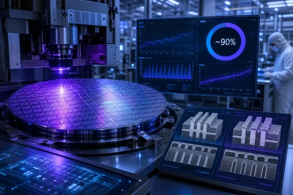
TSMC says its A14 process is moving through development faster than its N2 predecessor did at a comparable point, with internal test vehicles now nearing 90% of target device performance and roughly 90% yield on a 256Mb SRAM test structure. The update came during TSMC’s July 16 second-quarter 2026 earnings call, and was first detailed by Tom’s Hardware.
A14 is TSMC’s next major leading-edge node, scheduled for volume production in the second half of 2028. It uses the company’s second-generation gate-all-around nanosheet transistors, following N2 as TSMC’s first commercial GAA generation.
The latest figures improve on TSMC’s April update, when A14 had surpassed 85% of target device performance and 80% SRAM yield. TSMC CEO C.C. Wei described the program as on track, with both performance and SRAM-yield measures now close to 90%.
For context, N2 was reported to have exceeded 80% of its target device performance and 50% yield on the same class of 256Mb SRAM test chip in April 2023. By April 2024, N2 had passed 90% performance and 80% SRAM yield. The comparison is not exact—process programs, test vehicles, and design rules differ—but A14’s reported development curve is plainly stronger.
That matters because yield learning is one of the slowest and most expensive parts of bringing an advanced process node to volume. TSMC’s added experience with nanosheet transistors is the likely advantage: N2 introduced the company’s first GAA devices, while A14 builds on that work rather than starting from a new transistor architecture.
The SRAM result should not be read as a claim that early A14 CPUs, GPUs, or AI accelerators will ship with a 90% functional yield. SRAM arrays are highly repetitive structures used to judge defect density and process consistency. Commercial chips introduce larger dies, more varied logic, I/O, analog components, cache configurations, voltage targets, and customer-specific design choices.
TSMC has previously projected that A14 will offer a 10% to 15% speed gain at the same power versus N2, or a 25% to 30% reduction in power at the same speed, alongside roughly 20% higher chip density. Those are foundry-level targets, not guarantees for a particular Windows PC processor or graphics card.
For Windows users and IT buyers, A14 is a 2028-and-later roadmap signal rather than an imminent product change. The nearer question remains how N2 ramps through phones, PCs, GPUs, and AI hardware before A14 reaches volume production.
A14 is TSMC’s next major leading-edge node, scheduled for volume production in the second half of 2028. It uses the company’s second-generation gate-all-around nanosheet transistors, following N2 as TSMC’s first commercial GAA generation.
 A quicker ramp than N2
The latest figures improve on TSMC’s April update, when A14 had surpassed 85% of target device performance and 80% SRAM yield. TSMC CEO C.C. Wei described the program as on track, with both performance and SRAM-yield measures now close to 90%.For context, N2 was reported to have exceeded 80% of its target device performance and 50% yield on the same class of 256Mb SRAM test chip in April 2023. By April 2024, N2 had passed 90% performance and 80% SRAM yield. The comparison is not exact—process programs, test vehicles, and design rules differ—but A14’s reported development curve is plainly stronger.
That matters because yield learning is one of the slowest and most expensive parts of bringing an advanced process node to volume. TSMC’s added experience with nanosheet transistors is the likely advantage: N2 introduced the company’s first GAA devices, while A14 builds on that work rather than starting from a new transistor architecture.
The SRAM result should not be read as a claim that early A14 CPUs, GPUs, or AI accelerators will ship with a 90% functional yield. SRAM arrays are highly repetitive structures used to judge defect density and process consistency. Commercial chips introduce larger dies, more varied logic, I/O, analog components, cache configurations, voltage targets, and customer-specific design choices.
Smartphone and AI customers are already engaged
TSMC also said interest is strong across both smartphone and HPC/AI customers, with new A14 tape-outs reportedly running ahead of schedule. The company did not identify customers or products.TSMC has previously projected that A14 will offer a 10% to 15% speed gain at the same power versus N2, or a 25% to 30% reduction in power at the same speed, alongside roughly 20% higher chip density. Those are foundry-level targets, not guarantees for a particular Windows PC processor or graphics card.
For Windows users and IT buyers, A14 is a 2028-and-later roadmap signal rather than an imminent product change. The nearer question remains how N2 ramps through phones, PCs, GPUs, and AI hardware before A14 reaches volume production.
References
- Primary source: Tom's Hardware
Published: 2026-07-17T15:30:26+00:00
TSMC confirms significant yield and performance improvements in A14 update — strong interest from AI/HPC and smartphone customers | Tom's Hardware
Mass production ahead of schedule?www.tomshardware.com - Related coverage: tech.yahoo.com
TSMC confirms significant yield and performance improvements in A14 update — strong interest from AI/HPC an...
TSMC's A14 process technology progresses faster than N2 at this stage of development as developers of both client and AI/HPC plan to use it.tech.yahoo.com