
In a July 29 Intel Newsroom report, the company said its New Mexico operations can now support chip complexes exceeding eight times the conventional reticle limit—the maximum area a lithography system can expose in one shot—and target more than 12 times that limit by 2028. That scale matters to data-center AI designs that need large amounts of compute placed alongside high-bandwidth memory and I/O silicon.
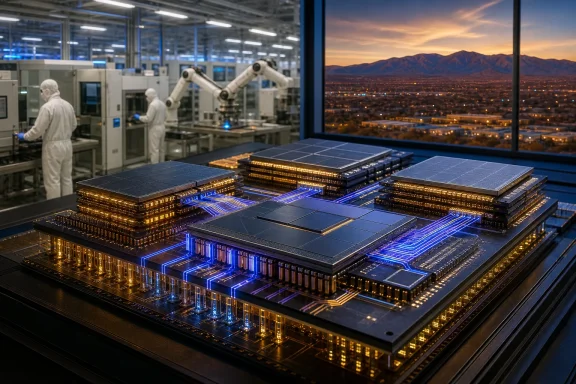 Packaging Is Becoming the AI System
For Windows users, advanced packaging is mostly invisible. But it increasingly determines the capabilities and power profile of the processors beneath AI PCs, workstations and cloud services: compute tiles can be manufactured on one process, memory interfaces on another, then combined into a tightly connected package.
Intel is positioning its Foveros and Embedded Multi-Die Interconnect Bridge, or EMIB, technologies as the mechanisms for that integration. Foveros provides vertical, three-dimensional die stacking, while EMIB uses small embedded silicon bridges to create short, high-bandwidth links between adjacent dies without requiring a full-package silicon interposer.
The result is a system of chips rather than a single huge chip. That gives designers more freedom to mix process nodes and functions, although it also makes thermal management, power delivery, test and manufacturing yield far more challenging.
EMIB-T Moves Power Through the Bridge
The newest element highlighted by Intel is EMIB-T, an evolution of EMIB that adds through-silicon vias to route power through the bridge as well as signals. Intel says this is intended to improve power delivery and signal routing for future high-bandwidth-memory configurations.
That focus is significant. Modern AI accelerators are often constrained less by raw arithmetic throughput than by moving data between compute, memory and networking components. A packaging platform that can accommodate more HBM stacks and sustain dense interconnects could become as strategically important as the transistor process used for the individual dies.
Intel previously described EMIB-T as part of its broader foundry roadmap, and the company has said it expects the technology to enter higher-volume customer ramps during the second half of 2026. The July report frames New Mexico as a central U.S. manufacturing base for that effort.
A Foundry Pitch Built Around Assembly
Intel’s New Mexico operation began as a wafer-manufacturing site in 1980 and now employs roughly 2,700 people, according to the Intel Newsroom report. Intel says the operation works with about 500 suppliers, illustrating that advanced packaging is not simply a final assembly step but a supply-chain-intensive manufacturing discipline.
For Intel Foundry, the message is equally commercial: customers may select a packaging technology first, then decide whether to use Intel for additional manufacturing. That is a different pitch from competing purely on leading-edge wafer nodes, particularly for companies designing heterogeneous AI systems whose components may originate on different processes or from different vendors.
Intel’s 2028 scale targets remain forward-looking claims, not shipping product specifications. Still, the near-term test will be whether EMIB-T and Foveros capacity translate into visible customer designs—and whether Intel can turn New Mexico’s packaging expertise into foundry orders as AI hardware shifts from bigger chips to bigger packages.
