
That is the useful conclusion behind New Electronics’ overview of changing foundry roles. Its account correctly identifies three connected shifts—gate-all-around transistors, advanced packaging and AI-assisted design and fabrication—but it understates the practical change for customers: a chip company can no longer treat the fab as a distant contract manufacturer once its product crosses a certain level of complexity. The package, the manufacturing rules and the available assembly capacity now shape the architecture before a design is finalized.
TSMC, Samsung Foundry and Intel Foundry all market versions of this broader service model. Their technical roadmaps differ, but the direction is shared: sell process technology together with the tools, packaging and validated flows needed to turn multiple dies into a working product.
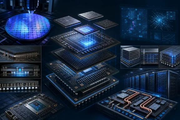 The leading node is only one part of the product
Moving from 3nm-class production toward 2nm-class processes remains important, particularly for dense CPU and accelerator logic where power efficiency and transistor density determine whether a design is viable. TSMC’s 2025 annual report says its 2nm technology entered volume production that year, while Samsung has positioned gate-all-around technology as central to its sub-3nm process plans. Intel’s 18A platform combines its RibbonFET gate-all-around transistor design with backside power delivery, branded PowerVia.
Gate-all-around, often shortened to GAA, changes the transistor structure so that the gate surrounds the channel more completely than in the FinFET designs that defined several previous generations. The intended benefit is tighter electrical control, which can help reduce leakage while preserving switching performance. That matters for high-density compute, where power delivery and heat have become limits every bit as real as transistor size.
But a node name alone no longer tells a customer enough about the resulting chip. A large AI processor may use the most advanced available logic for compute tiles, an older and cheaper process for I/O, specialized memory stacks from another supplier, and a package that determines how all of those pieces exchange data. The product’s performance, power use, cost and availability therefore depend on decisions that span several process generations and several companies.
This is where the conventional description of a foundry begins to fail. The foundry still fabricates wafers, but for high-end designs it also has to make the customer’s system partitioning manufacturable. That includes determining which functions belong on which dies, selecting the interconnect approach, validating thermal and electrical behavior, and planning test and assembly. Those decisions used to sit more cleanly with the chip designer or outsourced packaging houses. They now overlap.
Advanced packaging has become an architectural constraint
The most significant change is advanced packaging, not because chiplets are new, but because AI demand has made package-scale integration a mainstream performance requirement. TSMC’s CoWoS platform combines logic dies with high-bandwidth memory on an interposer-based package. Intel uses EMIB silicon bridges and Foveros stacking to link and vertically stack multiple dies. Samsung offers 2.5D and 3D heterogeneous-integration packaging alongside its wafer fabrication services.
These technologies allow designers to break a huge chip into smaller functional pieces. That can improve yield: a defect on a smaller compute die wastes less silicon than a defect on one giant monolithic die. It can also avoid putting every block on the costliest process node. Analog circuitry, I/O and some memory-related functions do not necessarily benefit from the same scaling as CPU or AI compute logic.
The headline claim that chiplets deliver better yields and flexibility needs a qualification, however. Chiplets move complexity; they do not erase it. The package has to carry immense bandwidth with low latency, route power without creating electrical or thermal failures, and survive assembly with acceptable yield. A product can gain manufacturing efficiency at die level while becoming harder and more expensive to assemble and test.
For enterprise buyers, this helps explain why the availability of AI systems cannot be understood simply by asking whether a fab has enough leading-edge wafers. An accelerator can be constrained by high-bandwidth memory, advanced package substrates, assembly capacity or package-test throughput. TSMC describes CoWoS as a foundation for high-performance computing and AI products, while Intel explicitly presents EMIB and Foveros as ways to build larger heterogeneous systems beyond a single reticle-sized die. Those are not side services; they are part of the manufacturing path for the products customers want to deploy.
The direct PC consequence will be gradual rather than dramatic. Consumer processors already use multi-die designs, and client devices are likely to adopt more specialized partitions as on-device AI, graphics, media processing and connectivity continue to diverge. The important change is that a future processor’s capabilities may be determined as much by its package design and die-to-die links as by the node used for its CPU cores.
Foundries are selling design enablement as well as capacity
A customer cannot take a set of chiplets to any factory and expect a working package. Each advanced packaging scheme has physical limits, routing rules, thermal constraints, supported memory configurations, design-kit requirements and test flows. The foundry that owns or controls those rules becomes involved earlier in the product-development cycle.
Intel Foundry has made this explicit with an “open chiplet” message built around the Universal Chiplet Interconnect Express, or UCIe, standard. UCIe can reduce the risk of proprietary die-to-die connections by defining a common interface, but it does not make all packages interchangeable. A standard describes how compatible dies communicate; it does not turn TSMC CoWoS, Intel EMIB/Foveros and Samsung’s packaging technologies into identical manufacturing services.
That distinction is commercially important. Open interfaces can give chip designers more component options, yet the most demanding products still need a specific physical package implementation. Customers are therefore buying a combination of intellectual-property libraries, electrical and thermal analysis, packaging choices, validation support and manufacturing capacity. A foundry’s customer relationship becomes closer and stickier, but the customer also becomes more dependent on that foundry’s roadmap and available capacity.
New Electronics calls this a move toward foundries becoming technology partners. That is directionally right, although “partner” should not obscure the power balance. A major foundry is not merely offering advice; it may control a bottleneck that determines whether the customer can ship a product at all. Design teams should treat process and packaging selection as supply-chain decisions from the start, rather than leaving packaging until the end of a tape-out program.
AI’s real role is data analysis, not autonomous fabs
The article also identifies AI as a growing tool in chip design and manufacturing. This is well supported in narrow, concrete areas. Inspection and metrology systems generate enormous quantities of wafer images and sensor data, and machine-learning methods can help identify defects, prioritize inspection and find correlations between process conditions and yield outcomes. ASML says its HMI inspection systems use machine learning for defect detection and inspection sampling, while its YieldStar metrology systems use AI to reduce time spent creating measurement recipes.
That is a more useful framing than the broad claim that AI “optimizes everything.” Semiconductor fabs have long used process-control software, statistical methods and automated equipment. The change is that ML models can process a larger number of variables and images faster, making them useful for anomaly detection, predictive maintenance and recipe tuning in a manufacturing process where a small drift can have expensive consequences.
AI-assisted materials research deserves an even sharper caveat. Matlantis promotes machine-learning interatomic-potential software for accelerating atomistic simulations and screening materials candidates before laboratory work. That may shorten early-stage research cycles, but it is not the same as proving that a candidate material will work in a commercial transistor, interconnect or package. Matlantis’ own educational documentation says its atomistic-simulation material does not cover electronic-structure analysis such as semiconductor band-gap analysis. Fast simulation can narrow the experimental search; it cannot replace fabrication, measurement and reliability qualification.
That limitation matters because new transistor structures and dense 3D packaging create materials problems that are often visible only after real process integration. A useful prediction is not that AI will eliminate trial-and-error in fabs, but that it will make failures easier to classify and reduce the number of unpromising experiments a manufacturer must run.
What changes for chip buyers and IT planners
For Windows and enterprise IT readers, the immediate lesson is to look past a processor’s process-node label. A platform’s actual value increasingly rests on package-level factors: memory bandwidth, accelerator-to-memory connectivity, power limits, cooling requirements, software support and the vendor’s ability to supply the complete part in volume.
That does not mean every PC buyer needs to study CoWoS, EMIB or gate-all-around transistor geometry. It does mean IT teams evaluating AI infrastructure should ask suppliers more specific questions:
- Does the proposed system depend on high-bandwidth-memory packages or other constrained assembly components?
- Are the CPU, accelerator, I/O and memory dies designed and qualified as a single package, or sourced through separate suppliers?
- What is the realistic service and replacement path if a package-level component is constrained?
- Does the claimed performance depend on a particular power envelope, cooling design or memory configuration that will not be present in the deployed system?
The old foundry model was defined by a relatively simple division of labor: designers created chips, fabs manufactured them, and packaging connected them to the outside world. That division is becoming less useful for the systems driving current demand. The foundry that can deliver leading-edge wafers but cannot provide the package, design support and production flow around them has an incomplete offering.
As 2nm-class logic, chiplet architectures and AI-assisted process control move from roadmaps into volume products, the competitive contest will be decided at the boundaries between dies as much as within them.
