
For Windows and PC readers, this remains an upstream story with a long lead time: no retail CPU, GPU, server accelerator, or Windows PC has been announced with a glass-core substrate. But the work matters because current organic package substrates are becoming a limiting factor for the enormous multi-die packages used by AI accelerators, high-end servers, and eventually the processors that filter into workstations and consumer PCs.
The significant update is less “glass is here” than the industry has finally entered the reliability gate. That is the point where suppliers must prove that a package will remain electrically and mechanically sound through thermal cycling, handling, assembly, and long-term operation. It is also the point where a series of optimistic glass-substrate schedules has repeatedly slipped.
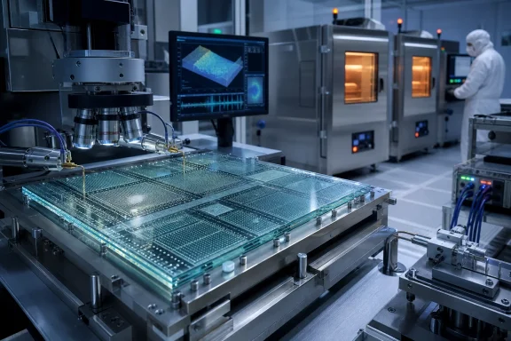 Absolics has samples in qualification, not a shipping product
Absolics, an SKC subsidiary, built its first U.S. glass-substrate facility in Covington, Georgia, around the promise that glass could replace the organic cores used in advanced semiconductor packaging. The project has substantial public backing: the Commerce Department awarded up to $75 million for the Georgia manufacturing effort, while the CHIPS National Advanced Packaging Manufacturing Program committed up to $100 million to a research partnership involving Absolics and Georgia Tech.
Those grants establish that the company is a serious participant in the U.S. advanced-packaging buildout. They do not establish commercial volume, named customers, qualification success, or a production design win. Absolics’ own public material describes its technology as having moved from concept to validation and highlights the federal awards, but it does not name an AMD, AWS, Nvidia, or other customer that has qualified glass cores for a product.
That distinction is vital. A substrate sample can meet internal electrical targets yet still fail packaging reliability, be too expensive to make at yield, or require changes to a customer’s assembly flow. The testing reportedly underway in Taiwan is therefore not a final administrative step. It is the test that determines whether Absolics can move from selling a technological possibility to supplying a repeatable manufacturing process.
The company’s proposed end-of-2026 mass-production target should be treated accordingly. It is an operating goal, not evidence that a commercial processor is imminent. The earlier schedule had placed volume production in the first half of 2024, illustrating how much harder it is to industrialize glass panels than to demonstrate their properties in controlled prototypes.
The hard problem is manufacturing a package, not making a glass panel
Intel’s original case for glass was compelling. The company said glass cores could enable substantially higher interconnect density than organic substrates, reduce pattern distortion, and improve dimensional stability as package sizes grow. Glass can be engineered with a coefficient of thermal expansion closer to silicon than conventional organic material, helping control warpage—the bending and deformation that becomes increasingly difficult to manage as packages get physically larger.
The payoff is especially relevant to chiplets. Rather than placing one monolithic silicon die in a package, modern server CPUs and AI accelerators can combine compute dies, I/O dies, cache, high-bandwidth memory, and networking components. That arrangement increases the amount of wiring and the physical area needed beneath the silicon. A stable glass core could support denser routing while allowing package makers to use rectangular panels more efficiently than circular silicon wafers for very large designs.
Yet those benefits create the manufacturing challenge. Glass is vulnerable to edge damage, cracking during drilling and singulation, and stress caused by the different materials layered above and below it. Through-glass vias—the microscopic vertical connections through the substrate—must be drilled and metallized with extremely high yield. Manufacturers must also maintain very tight flatness over panels roughly half a meter across, because minor variation can become a defect when dense redistribution layers and large silicon dies are added.
Intel’s more recent patent filings reinforce that these are not merely theoretical concerns. A March 2026 published application describes a glass-containing substrate with an edge-sealant structure intended to protect the lateral edges. That does not prove a manufacturing solution has been completed, but it is a useful indicator of where engineering work remains concentrated: preventing glass-edge failures rather than simply improving a data-sheet performance number.
For system builders, this means glass substrates should not be viewed as a drop-in replacement for today’s package boards. Their arrival requires equipment, materials, panel handling, inspection, drilling, metallization, and assembly practices to mature together. A reliable glass panel alone is insufficient if it cannot survive the rest of the packaging line at an acceptable yield.
Samsung’s joint venture is real, but its production date is not a product launch
Samsung Electro-Mechanics and Sumitomo Chemical’s Dongwoo Fine-Chem signed an agreement on July 2 to establish a glass-core joint venture provisionally called GlaSSEM. Samsung’s own regulatory disclosure confirms the central facts: the venture is planned with capital of 482.1 billion won, Samsung Electro-Mechanics will hold 66.2%, and Dongwoo Fine-Chem will hold the remaining stake. Samsung’s scheduled acquisition date is September 1, 2026, subject to the structure described in the filing.
That is a concrete commercial commitment, not a research memorandum. The new company is intended to manufacture and sell glass cores, giving Samsung Electro-Mechanics access to Dongwoo and Sumitomo’s materials experience while Samsung contributes substrate design and manufacturing capability.
But the formal disclosures do not make the same thing as a product announcement. Reporting cited by Tom’s Hardware places the targeted start of plant operations in the second half of 2027, while Samsung and Sumitomo’s public announcement says the venture itself is planned to be established in 2026 after required procedures. Neither company has announced a qualified processor package, a named customer, or a shipping product tied to the joint venture.
In other words, Samsung has made the supply-chain decision. It has not yet shown that its glass core is qualified for a customer’s package. The difference between a legally capitalized materials venture and a substrate beneath a working AMD, Broadcom, Nvidia, or Intel product can amount to years of process and reliability work.
Intel’s Lens partnership is more concrete than the “talks” description suggests
Intel began publicly promoting glass substrates in September 2023, saying it expected to bring complete glass-substrate solutions to market in the second half of the decade. Since then, Intel has shown test vehicles and continued to promote glass in its foundry material, including designs that combine glass with advanced package interconnect technologies such as EMIB.
At NEPCON Japan in January 2026, Intel Foundry demonstrated a thick-core glass substrate with embedded EMIB bridge dies, according to TrendForce. Intel said the test vehicle supported silicon around twice the reticle size and had not shown micro-cracking in the company’s testing. That is progress, but it remains a demonstration vehicle rather than an announced processor or accelerator program.
There is also a notable discrepancy in the current reporting around Intel’s relationship with Lens Technology. Tom’s Hardware described Intel as being in early talks with the Chinese cover-glass manufacturer and said no solid agreement had been reached. Intel’s own July 24 newsroom announcement, however, says the companies had already entered a strategic collaboration to explore advanced semiconductor-packaging technologies, including glass-substrate solutions.
The official announcement does not promise a production deal, volume target, or a specific Intel product. It does establish that the relationship had progressed beyond unconfirmed discussions by late July. Readers should interpret it as a development partnership intended to solve manufacturing and process problems, not as evidence that Intel has outsourced or licensed a commercial glass-substrate platform.
Intel’s public position is still consistent with a longer horizon than its 2023 messaging implied. The company has working samples and active partners, but no disclosed high-volume manufacturing program or product timetable. The practical read is that Intel is preserving options: developing its own glass-substrate technology, demonstrating it to foundry customers, and collaborating with specialty-glass manufacturing expertise while the industry searches for a manufacturable process.
The first verified design win is the milestone that matters
Several companies now have credible glass-substrate programs, including Absolics, Samsung Electro-Mechanics, LG Innotek, Japanese materials and printing companies, and Intel. TSMC is also expanding panel-level packaging work, though its use of glass cores remains less defined in public disclosures. A growing supplier list makes glass a legitimate packaging direction; it does not make it a deployed standard.
The industry’s next meaningful proof point will be an officially named customer and product, accompanied by a clear manufacturing claim. “Sample shipments,” “pilot-line operation,” “technology readiness,” and “final qualification” all describe steps before that point. The same caution applies to reports associating AMD, AWS, Broadcom, or Nvidia with particular glass-substrate suppliers: none of those companies has publicly announced a production product built on a glass core.
Absolics’ reliability data, expected before the end of 2026 if the current schedule holds, is the nearest tangible test. A successful result would not put glass into Windows PCs next year, but it would remove one of the biggest barriers between laboratory-scale panels and the supply chain for future AI servers, high-end workstations, and chiplet-heavy processors.