
For Windows users, PC builders, AI enthusiasts, and anyone watching the silicon supply chain, this is not simply a university-equipment purchase. It is a signal that advanced packaging, photonics, heterogeneous chiplets, and specialized accelerators are becoming just as important to the future of computing as traditional transistor scaling. The MBX is not positioned as a direct substitute for extreme ultraviolet lithography in the highest-volume CPU, GPU, DRAM, or smartphone SoC fabs. Instead, it targets an increasingly valuable gap: the work between a promising chip design and a manufacturable device.
That gap is where semiconductor projects can lose months, consume large mask budgets, and become trapped in a cycle of slow design revisions. Multibeam’s pitch is straightforward: remove the mask from the first stages of chip development, write patterns directly to wafers with multiple electron-beam columns operating in parallel, and let engineers test more designs before committing to conventional volume manufacturing.
 Background: Why Maskless Lithography Is Back in the Spotlight
Semiconductor lithography is the process used to transfer circuit patterns onto a wafer. In conventional optical lithography, light passes through or reflects from a patterned photomask—also called a reticle—to expose selected areas of a light-sensitive resist. The pattern is then developed and transferred through further deposition, etching, implantation, and cleaning steps.
That workflow is extraordinarily capable. It is also optimized for repeating the same mature pattern across huge numbers of wafers. When millions of identical chips are required, a mask’s cost can be distributed across an enormous production run. But when a device is still being refined, a mask can become a costly and time-consuming commitment.
A revised circuit layout may require a revised mask. A change to a packaging interconnect layer may require another mask. A research team comparing several possible chiplet connections, photonic waveguides, sensor patterns, or quantum-device structures can quickly face a substantial iteration burden before it has even determined which architecture is worth scaling.
Electron-beam lithography, or EBL, offers a different model. Instead of using light and a fixed mask, it writes patterns directly with an electron beam under software control. This makes it highly flexible: change the design data and the pattern can change without waiting for a new photomask. The longstanding problem is speed. Conventional EBL commonly uses one focused beam, writing features sequentially; the excellent resolution comes with a serious throughput penalty. Semiconductor analyst Mark LaPedus’ overview of the MBX launch
The economics have therefore kept direct-write e-beam tools concentrated in research, mask making, very low-volume production, and unusual device categories. Historical research into maskless lithography has repeatedly identified throughput—not basic resolution—as the central barrier to wider adoption. A review of maskless electron-beam lithography
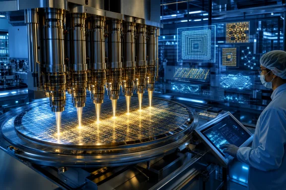
Multibeam’s technology is built around the argument that this tradeoff is not fixed. Rather than relying on one beam and one column, its platform uses an array of miniature electron-beam columns so that patterns can be written in parallel across a wafer. The company describes this approach as multi-column electron-beam lithography, or MEBL. Multibeam’s MBX platform description
That distinction matters. A maskless lithography tool that is merely more precise is useful in a laboratory. A maskless lithography tool that can improve the speed of repeated wafer-scale experimentation could have a much broader effect on semiconductor development cycles.
What NTHU Has Ordered
National Tsing Hua University, generally known as NTHU, has ordered Multibeam’s second-generation MBX platform for the university’s College of Semiconductor Research, or CoSR. The tool will be installed in a new facility and is intended to support university research alongside joint development projects with Taiwanese chipmakers. Multibeam says the system is due to ship in 2027, making it the company’s first deployment in Taiwan. The company’s order announcement
The reported use cases are telling. NTHU plans to use the tool for advanced chip-integration process development, including:
- Chip-first packaging, where dies are handled before later package layers are formed.
- Chip-last packaging, where interconnect and redistribution structures can be produced ahead of die placement.
- Large-format interposers, used to connect multiple chips within advanced packages.
- High-density chip-to-chip interconnect layers, increasingly essential for chiplets and high-bandwidth computing architectures.
- Research spanning advanced packaging, photonics, and quantum computing. Multibeam’s description of the planned NTHU deployment
This is a strategically sensible match for a university semiconductor program. NTHU’s College of Semiconductor Research was created as part of Taiwan’s broader effort to increase high-level semiconductor talent and strengthen industry-academia collaboration. Taiwan’s Ministry of Education says the college is one of six semiconductor research institutions established under a national framework intended to combine university education with corporate and government participation. Taiwan Ministry of Education overview (english.moe.gov.tw)
CoSR is located in Hsinchu, a city closely associated with Taiwan’s semiconductor ecosystem. Its formal mandate includes research, graduate education, and relationships with industry partners, making it an appropriate site for a tool whose value proposition is based on rapid movement from prototype to production-relevant process learning. NTHU College of Semiconductor Research information (cosr.site.nthu.edu.tw)
A First Taiwan Installation Carries More Weight Than a Typical Sale
Taiwan is not simply another destination for a lithography platform. It is a dense concentration of semiconductor manufacturing expertise, materials suppliers, packaging specialists, foundries, equipment engineers, and university research institutions. Multibeam will be placing its tool where its claims can be evaluated by organizations that understand semiconductor process integration at a very high level.
That is an opportunity, but also a demanding test. An installation in Taiwan can provide Multibeam with closer access to potential customers and collaborators in advanced packaging. At the same time, it increases the pressure to demonstrate reliable wafer handling, accurate pattern placement, repeatable process control, service support, and real economic value beyond a compelling technical concept.
The order should therefore be viewed as an important commercial validation point—not final proof that multi-column direct-write lithography has solved the industry’s throughput challenge across all applications.
How the MBX Approach Changes the Prototyping Workflow
The MBX’s practical appeal begins with the removal of mask fabrication from the earliest design cycles.
In a conventional flow, an engineer finishes a layout, sends data for mask creation, waits for mask preparation and qualification, runs a wafer, performs electrical and physical analysis, and then starts again if the results indicate a design or process adjustment. Each cycle has dependencies. Some are technical; others are logistical.
A direct-write system compresses that sequence:
- Engineers complete or modify the layout data.
- The pattern is prepared for the electron-beam writing process.
- The tool writes directly onto the resist-coated substrate.
- The wafer moves through development and subsequent process steps.
- The resulting structures can be characterized and compared against other variants.
The critical benefit is not that physics becomes simpler. Semiconductor manufacturing remains complicated, and every downstream deposition, etch, metrology, bonding, and reliability step still matters. The benefit is that a design change does not automatically trigger a new photomask order.
Multibeam says its MBX-300 family is designed to support rapid design modification without mask respins, multiple experiments on a single substrate, and a path from development through pilot production. The company also lists support for 150 mm, 200 mm, and 300 mm wafers, plus 310 mm panels, and materials including silicon, indium phosphide, gallium nitride, silicon carbide, gallium arsenide, and glass. Multibeam’s published MBX-300 specifications and application overview
For chip researchers, this can create a different style of experimentation. Instead of building a wafer around one frozen design, a team can place multiple variations on the same substrate. That could mean different interconnect pitches, routing geometries, photonic grating structures, transistor layouts, quantum-device patterns, or package-level signal paths.
The outcome is a tighter design-fabricate-measure-learn loop. That loop is especially valuable in sectors where architecture remains fluid and manufacturing knowledge is still being developed.
Why Advanced Packaging Is a Logical Starting Point
The semiconductor industry’s center of gravity is moving beyond monolithic chips. A modern computing package may combine compute dies, memory stacks, I/O dies, networking components, accelerators, and specialized analog or photonic elements. This shift makes advanced packaging a design and manufacturing discipline in its own right rather than a final assembly step.
Interposers and redistribution layers are central to that evolution. They provide electrical pathways among dies and external connections, often with demanding density, alignment, and topography requirements. As architectures become more customized, the value of flexible direct-write patterning grows.
Multibeam explicitly identifies high-density interconnect patterning, 2.5D integration, 3D integration, and heterogeneous integration as MBX applications. Multibeam’s advanced-packaging use-case description
This is why the announcement has relevance to future Windows PCs and data-center systems even if the MBX never prints the leading-edge transistor layers of a mass-market x86 processor. The next generation of AI PCs, GPUs, servers, and high-performance accelerators will increasingly depend on packaging technologies that connect specialized components efficiently. Improving the speed at which those package architectures can be tested may ultimately influence product design choices upstream.
The Strengths of Multi-Column E-Beam Lithography
The potential strengths of the MBX platform are substantial, particularly for the right workload.
Faster Iteration Without a Mask Queue
The most obvious advantage is maskless flexibility. Direct-write patterning enables a wafer to reflect the current design database rather than the design frozen when a photomask was ordered. That is useful where design revisions are frequent and product volumes initially remain limited.
For startups, university labs, defense-oriented programs, photonics teams, quantum-device researchers, and custom accelerator developers, the ability to avoid repeated mask cycles could reduce the financial and scheduling friction that normally separates a new concept from a functional test vehicle.
Parallel Beams Address EBL’s Historic Weakness
Multibeam’s essential technical claim is that an array of independently controlled miniature columns writes in parallel, addressing the serial nature of conventional single-beam EBL. Semiecosystem’s launch coverage
Parallelism is the correct direction for improving direct-write throughput. Industry roadmaps have long recognized multi-column electron-beam approaches as a possible route toward faster maskless patterning, particularly for applications such as 3D packaging and MEMS. IEEE’s International Roadmap for Devices and Systems lithography chapter
The key difference between a research demonstration and a manufacturable system, however, is whether every beam can remain controlled, calibrated, and synchronized across a real wafer and across repeated lots.
Broad Substrate and Material Support
The MBX platform’s claimed support for wafer sizes ranging through 300 mm and for materials beyond silicon is an important differentiator. Silicon photonics, compound semiconductors, power electronics, and some quantum-device programs can require materials and device forms that do not map neatly to the most standardized leading-edge CMOS workflows. Multibeam’s materials and substrate-format list
This flexibility could be particularly useful where a team needs to experiment with non-silicon materials or hybrid stacks while also moving toward a production-capable process.
A More Continuous Prototype-to-Production Path
Multibeam’s earlier platform has already been delivered to U.S. foundry operator SkyWater Technology. SkyWater said in July 2024 that it had received a multicolumn e-beam system intended for rapid prototyping and production applications, including secure chip identification, large-format die, microfluidics, MEMS, photonics, and high-density devices. SkyWater’s deployment announcement
That installed-base experience is meaningful because it moves the technology discussion beyond a newly announced platform. SkyWater’s use also illustrates Multibeam’s actual market focus: specialized, high-mix, and unusual applications where flexibility can outweigh the raw wafer-per-hour advantage of conventional optical lithography.
The Risks: Throughput Is Only One Part of the Challenge
The MBX order is encouraging, but semiconductor equipment claims need to be assessed carefully. Faster than a conventional e-beam system does not automatically mean competitive with every optical lithography workflow.
“High Productivity” Needs Application-Specific Context
Multibeam describes the MBX as enabling direct-write manufacturing at production-relevant throughput levels. Multibeam’s platform page Yet public materials currently emphasize applications and workflow benefits more than universally comparable specifications such as verified wafers per hour, overlay accuracy, uptime, defect density, and cost of ownership for defined layers.
That does not undermine the NTHU deployment. It does mean readers should avoid interpreting “production” as shorthand for replacing an EUV scanner or high-volume DUV line in the most advanced logic fab. Production is not a single category. A tool can be production-relevant and economically compelling for a high-mix photonics or packaging flow while remaining unsuitable for commodity high-volume processor manufacturing.
Independent launch coverage also reports that Multibeam is targeting specialty applications rather than leading-edge logic and memory. Semiecosystem’s report on MBX market positioning
Multi-Beam Control Is a Complex Engineering Problem
Adding beams increases parallelism, but it also increases control complexity. Every beam column needs stable performance. Beam-to-beam uniformity, writing-field alignment, stage accuracy, distortion control, charge effects, resist behavior, and stitching between writing regions can all affect pattern fidelity.
These are not trivial implementation details. The more complex the device and the larger the wafer area, the more difficult it becomes to maintain consistent critical dimensions and placement accuracy everywhere that matters.
The International Roadmap for Devices and Systems identifies topography, alignment, overlay, yield, cost, and defectivity as major lithography challenges for increasingly complex three-dimensional stacks. IEEE IRDS lithography roadmap
For NTHU, this is precisely why the system is valuable as a research asset. It creates an environment in which the university and industry collaborators can evaluate those tradeoffs in real process-development work rather than treating maskless lithography as an abstract promise.
The Tool Must Prove Operational Reliability
A lithography platform does not earn adoption solely through attractive patterning results. Fabs will evaluate serviceability, uptime, software integration, process repeatability, recipe management, contamination controls, training requirements, and the ability to integrate with metrology and downstream process equipment.
Multibeam’s first SkyWater deployment is relevant because the company said the collaboration informed the tool’s fab-operational specifications. SkyWater’s account of the development partnership The NTHU installation will provide another important operating environment, this time inside a leading Asian semiconductor research ecosystem.
The system’s success will be measured less by launch language and more by how rapidly researchers can run repeatable experiments, how easily industrial partners can translate results into their own flows, and whether the platform reduces the total cycle time of process development.
Why This Matters for the Future of AI PCs and Windows Hardware
The most immediate beneficiaries of faster semiconductor prototyping may not be mainstream CPU makers. They are more likely to be the teams building devices that conventional high-volume flows do not serve efficiently: custom AI accelerators, silicon photonics modules, advanced sensor arrays, secure processors, specialty power devices, and quantum hardware.
But these categories increasingly intersect with the Windows ecosystem.
AI PCs require more than a capable CPU. They combine GPUs, NPUs, memory, storage, networking, power-management components, and ever more sophisticated packaging. Data centers supporting Windows workloads, cloud AI services, developer tools, enterprise applications, and consumer AI features require even denser and more power-efficient accelerator systems.
The next leap in computing performance may therefore come from how chips are assembled and connected, not solely from how small an individual transistor can become. Heterogeneous integration enables designers to combine components optimized for different tasks instead of forcing every function onto one enormous monolithic die.
Maskless, multi-column EBL could help shorten the trial-and-error phase for those systems. It may make it easier to test an experimental interposer, a revised chiplet link, a different photonic interface, or a packaging change that improves bandwidth or power efficiency. The value is not merely making a prototype faster; it is enabling more candidate designs to exist before the final architecture is locked.
The Larger Significance of the NTHU Deal
NTHU’s MBX purchase is best understood as a vote of confidence in a particular development model: faster learning through flexible wafer-level experimentation.
The company is not claiming that photomasks will disappear. They will remain central to the enormous-volume production of standardized chips. Optical lithography—especially advanced DUV and EUV—continues to be the industrial foundation for the most demanding leading-edge logic and memory manufacturing.
What is changing is the importance of applications that do not fit that model perfectly. Advanced packaging, chiplets, photonics, quantum systems, compound semiconductors, MEMS, and custom AI hardware all reward flexibility. They also benefit from faster iteration because their architectures, materials, and manufacturing methods are evolving quickly.
Multibeam’s MBX platform is attempting to make e-beam lithography practical in that zone between research-only patterning and mature, massively replicated chip production. Its promise is compelling: fewer mask-dependent delays, more design variants per wafer, and a more direct route from concept to process qualification.
The Taiwan installation will not settle every question about multi-column electron-beam lithography. But it will put the technology in front of exactly the kind of researchers and industrial partners who can determine where it delivers genuine advantages. If the system performs as intended, the impact may be felt first in specialized devices and advanced packaging—and then, indirectly, in the hardware architectures that shape the next generation of Windows PCs, AI workstations, and data-center platforms.
