
The Elec, citing semiconductor-industry sources, reported August 24 that KCTech is the sole supplier selected for the equipment-and-materials package and that shipments could begin in the fourth quarter of 2026. KCTech declined to confirm customer matters when contacted by the publication. No public purchase order, installation schedule, unit count, or contract value has been disclosed by KCTech, Absolics, or parent company SKC.
That distinction is important. The reported deal is a meaningful sign that Absolics is adding process capability needed for commercial glass substrates, but it is not confirmation that high-volume production has begun. SKC’s own recent disclosures still describe the Georgia operation as moving through customer qualification, prototype output, yield improvement, and mass-production preparation.
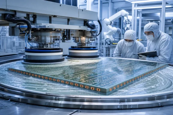 CMP is the process glass packaging cannot simply skip
Chemical-mechanical polishing, or CMP, combines abrasive slurry with a polishing pad and controlled pressure to remove material evenly and leave a highly planar surface. It is a mature step in silicon wafer fabrication, but applying it to large glass panels used in advanced packaging is a different manufacturing problem.
Absolics is developing glass-core package substrates that use through-glass vias, or TGVs: microscopic passages drilled through the glass and filled with copper to connect circuitry on opposite sides. After copper plating, excess metal and topographical variation remain across the panel. Wet etching can remove some unwanted copper, but it is less suited to bringing copper and glass to a tightly controlled common height over a large area.
For fine redistribution layers — the dense copper wiring that routes signals among chiplets and other components in a package — surface variation is a yield risk. A substrate that is not sufficiently flat can complicate subsequent lithography, metal deposition, dielectric coating, and bonding steps. CMP is therefore not a cosmetic finishing operation; it is a process intended to make later high-density interconnect steps repeatable.
Intel has made the broader technical case for glass substrates, saying the material can offer better dimensional stability and lower distortion than conventional organic substrates. Intel’s glass work remains aimed at products later this decade, underscoring the gap between demonstrating promising material properties and running a reliable, cost-effective manufacturing flow at scale.
The difficult part for Absolics is not merely proving that copper-filled glass vias can be made. It is producing panel after panel with uniform planarity, controlled defects, acceptable throughput, and yields that customers will accept for expensive AI, networking, graphics, and high-performance computing packages.
The equipment order is more revealing than the reported price
The Elec reported that each KCTech CMP system for Absolics may cost roughly 7 billion to 8 billion won, placing it in the range of high-end semiconductor CMP tools. That estimate has not been independently confirmed, and the number of systems Absolics may install is unknown.
The more consequential element is the reported pairing of the tool with KCTech’s slurry. CMP performance comes from the interaction of the machine, polishing pad, slurry chemistry, pressure, motion profile, endpoint controls, and cleaning sequence. Buying equipment and slurry from the same supplier can shorten process integration work because the chemical and mechanical sides are developed together. It can also concentrate operational dependence on one vendor during the early production ramp.
KCTech publicly lists both CMP equipment and CMP slurry among its semiconductor products. The company has an established business in wafer CMP, but the Absolics program would extend that work into a substantially larger panel format and a packaging-specific copper-and-glass process. The Elec previously reported that KCTech had developed CMP equipment for 510-by-515-millimeter glass substrates, a size that has emerged as a practical target for panel-level packaging development.
Large panels change the economics and the engineering. A 510-by-515-mm panel has far more usable area than a 300-mm wafer, which is attractive for packaging many devices at once. But any nonuniformity is also spread over a larger surface. Removing thick copper evenly across a square glass panel without scratching, cracking, edge chipping, dishing copper features, or producing uneven removal rates is a demanding integration problem.
KCTech’s reported role therefore points to a less visible reality of glass-substrate commercialization: success depends as much on specialized process equipment and consumables as on the glass itself. A material can have excellent thermal and mechanical properties in a lab and still fail to become a viable package substrate if its manufacturing flow is slow, inconsistent, or too expensive.
Absolics is buying capability while qualification remains unfinished
Absolics is SKC’s U.S.-based glass-substrate subsidiary, with its main manufacturing site in Covington. The U.S. Department of Commerce announced preliminary CHIPS Act terms in May 2024 for up to $75 million in direct funding to support Absolics’ glass-substrate technology and facility, calling it the first proposed CHIPS investment in a commercial facility making a new advanced material for the semiconductor supply chain.
SKC has since said its Georgia facility was completed and producing prototypes, while its public materials continued to frame commercialization as a work in progress. In August 2026, Seoul Economic Daily reported that SKC was injecting 401.1 billion won into Absolics for testing, customer certification, and improvements to yield and quality. According to that reporting, embedded-glass product samples had moved into reliability testing after preliminary evaluation, while another product path was still awaiting supplier-selection and proof-of-concept milestones.
Those details put the KCTech report in context. A CMP-tool shipment in the fourth quarter would fit a factory preparing to harden its manufacturing flow during qualification. It would not, by itself, signal that customers have signed off on commercial volumes or that the factory’s process yields are stable.
SKC has revised timing around glass-substrate commercialization before as customer requirements added validation work. That history makes the missing details in the KCTech report especially material: there is no stated installation date, no stated acceptance-test milestone, no capacity target tied to the tools, and no indication of when a qualified customer would receive production parts.
For IT buyers and infrastructure planners, this remains a supply-chain development rather than a product roadmap event. No processor vendor has announced a commercially shipping server, accelerator, or PC platform using Absolics glass substrates, and Intel’s own public glass-substrate timeline still points to the latter half of the decade.
Why a consumables contract could matter more over time
CMP tools are capital purchases made when a manufacturing line is equipped or expanded. Slurry is consumed continuously as panels are processed. If Absolics moves from prototypes to sustained production, the slurry side of the reported KCTech arrangement could become the more durable revenue stream.
That is also why the “sole supplier” assertion deserves caution. Sole-source arrangements can help a new process come up faster because one company owns more of the recipe and troubleshooting loop. They can also create a bottleneck if a consumable must be qualified again, a formulation changes, or output rises faster than the supplier’s capacity. The Elec’s reporting establishes the claimed selection, but neither company has publicly described the qualification terms, dual-sourcing plans, service footprint in Georgia, or the supply commitments behind it.
The next meaningful confirmation will not be an equipment shipment alone. It will be evidence that Absolics can use CMP to meet customer reliability and yield targets on production-representative glass panels. Until then, KCTech’s reported order should be read as a concrete factory-readiness step — and a reminder that glass-core packaging depends on mastering planarization at industrial scale, not simply on replacing an organic substrate with glass.
